Ion-Beam Sputtering Deposited Cu-Doped CdS Thin Film

Article Preview

Abstract:

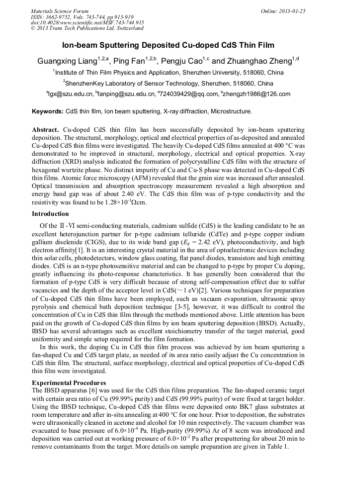
Cu-doped CdS thin film has been successfully deposited by ion-beam sputtering deposition. The structural, morphology, optical and electrical properties of as-deposited and annealed Cu-doped CdS thin films were investigated. The heavily Cu-doped CdS films annealed at 400 °C was demonstrated to be improved in structural, morphology, electrical and optical properties. X-ray diffraction (XRD) analysis indicated the formation of polycrystalline CdS film with the structure of hexagonal wurtzite phase. No distinct impurity of Cu and Cu-S phase was detected in Cu-doped CdS thin films. Atomic force microscopy (AFM) revealed that the grain size was increased after annealed. Optical transmission and absorption spectroscopy measurement revealed a high absorption and energy band gap was of about 2.40 eV. The CdS thin film was of p-type conductivity and the resistivity was found to be 1.28×10⁻¹Ωcm.

You might also be interested in these eBooks

Info:

Periodical:

Materials Science Forum (Volumes 743-744)

Pages:

915-919

Citation:

Online since:

January 2013

Export:

Price:

Permissions CCC:

Permissions PLS:

Сopyright:

© 2013 Trans Tech Publications Ltd. All Rights Reserved

Share:

Citation:

[1] I. Oladeji, L. Chow, C. Ferekides, V. Viswanathan, et al., Metal/CdTe/CdS/Cd1-xZnxS/TCO/Glass: A New CdTe Thin Film Solar Cell Structure. Sol. Energy Mater. Sol. Cells., 61 (2000) 203.

DOI: 10.1016/s0927-0248(99)00114-2

Google Scholar

[2] H.K. Xie, C.J. Tian, W Lei, et al., Preparation of p-type CdS thin films and in situ dark conductivity in vacuum deposited CdS: Cu films. Appl. Surf. Sci., 257 (2010) 1623-1627.

DOI: 10.1016/j.apsusc.2010.08.110

Google Scholar

[3] S. Kose, F. Atay, V. Bilgin, I. Akyuz, et al., Optical characterization and determination of carrier density of ultrasonically sprayed CdS: Cu films. Appl. Surf. Sci., 256 (2010) 4299-4303.

DOI: 10.1016/j.apsusc.2010.02.018

Google Scholar

[4] Y. Kashiwaba, I. Kanno and T. Ikeda, p-Type characteristics of Cu-doped CdS thin films. Jpn. J. Appl. Phys., 31 (1992) 1170-1175.

DOI: 10.1143/jjap.31.1170

Google Scholar

[5] P.J. Sebastianm, p-Type CdS thin films formed by in situ Cu doping in the chemical bath. Appl Phys Lett., 15 (1993) 2956-2958.

DOI: 10.1063/1.109181

Google Scholar

[6] P. Fan, G.X. Liang, X. M Cai, et al., The influence of annealing temperature on the structural, electrical and optical properties of ion beam sputtered CuInSe, Thin Solid Films, 519 (2011) 5348.

DOI: 10.1016/j.tsf.2011.02.036

Google Scholar

[7] A.S. Khomane, Morphological and opto-electronic characterization of chemically deposited cadmium sulphide thin films, J. Alloys Compd., 496 (2010) 508-511.

DOI: 10.1016/j.jallcom.2010.02.090

Google Scholar