p.653
p.657
p.661
p.665
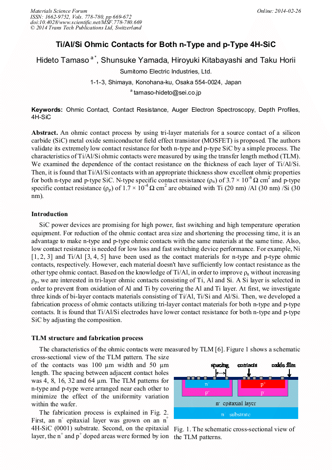
p.669
p.673
p.677
p.681
p.685
Ti/Al/Si Ohmic Contacts for both n-Type and p-Type 4H-SiC

Abstract:
An ohmic contact process by using tri-layer materials for a source contact of a silicon carbide (SiC) metal oxide semiconductor field effect transistor (MOSFET) is proposed. The authors validate its extremely low contact resistance for both n-type and p-type SiC by a simple process. The characteristics of Ti/Al/Si ohmic contacts were measured by using the transfer length method (TLM). We examined the dependence of the contact resistance on the thickness of each layer of Ti/Al/Si. Then, it is found that Ti/Al/Si contacts with an appropriate thickness show excellent ohmic properties for both n-type and p-type SiC. N-type specific contact resistance (ρn) of 3.7 × 10⁻⁶ Ω cm2 and p-type specific contact resistance (ρp) of 1.7 × 10⁻⁴ Ω cm2 are obtained with Ti (20 nm) /Al (30 nm) /Si (30 nm).
Info:
Periodical:
Pages:
669-672
Citation:
Online since:
February 2014
Authors:
Price:
Сopyright:
© 2014 Trans Tech Publications Ltd. All Rights Reserved
Share:
Citation: