III-V/Ge Device Engineering for CMOS Photonics

Article Preview

Abstract:

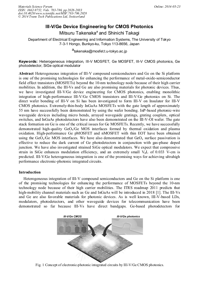
Heterogeneous integration of III-V compound semiconductors and Ge on the Si platform is one of the promising technologies for enhancing the performance of metal-oxide-semiconductor field effect transistors (MOSFETs) beyond the 10-nm technology node because of their high carrier mobilities. In addition, the III-Vs and Ge are also promising materials for photonic devices. Thus, we have investigated III-V/Ge device engineering for CMOS photonics, enabling monolithic integration of high-performance III-V/Ge CMOS transistors and III-V/Ge photonics on Si. The direct wafer bonding of III-V on Si has been investigated to form III-V on Insulator for III-V CMOS photonics. Extremely-thin-body InGaAs MOSFETs with the gate length of approximately 55 nm have successfully been demonstrated by using the wafer bonding. InP-based photonic-wire waveguide devices including micro bends, arrayed waveguide gratings, grating couplers, optical switches, and InGaAs photodetectors have also been demonstrated on the III-V-OI wafer. The gate stack formation on Ge is one of the critical issues for Ge MOSFETs. Recently, we have successfully demonstrated high-quality GeOx/Ge MOS interfaces formed by thermal oxidation and plasma oxidation. High-performance Ge pMOSFET and nMOSFET with thin EOT have been obtained using the GeOx/Ge MOS interfaces. We have also demonstrated that GeOx surface passivation is effective to reduce the dark current of Ge photodetectors in conjunction with gas-phase doped junction. We have also investigated strained SiGe optical modulators. We expect that compressive strain in SiGe enhances modulation efficiency, and an extremely small VπL of 0.033 V-cm is predicted. III-V/Ge heterogeneous integration is one of the promising ways for achieving ultrahigh performance electronic-photonic integrated circuits.

You might also be interested in these eBooks

Info:

Periodical:

Materials Science Forum (Volumes 783-786)

Pages:

2028-2033

Citation:

Online since:

May 2014

Export:

Price:

Permissions CCC:

Permissions PLS:

Сopyright:

© 2014 Trans Tech Publications Ltd. All Rights Reserved

Share:

Citation:

* - Corresponding Author

[1] Information on http: /www. itrs. net.

Google Scholar

[2] M. Takenaka and Y. Nakano, Optics Express Letters, 15 (2007) 8422-8427.

Google Scholar

[3] R. Suzuki, N. Taoka, M. Yokoyama, S. Lee, S. H. Kim, T. Hoshii, T. Yasuda, W. Jevasuwan, T. Maeda, O. Ichikawa, N. Fukuhara, M. Hata, M. Takenaka, and S. Takagi, Appl. Phys. Lett., 100 (2012) 132906.

DOI: 10.1063/1.3698095

Google Scholar

[4] M. Yokoyama, T. Yasuda, H. Takagi, H. Yamada, N. Fukuhara, M. Hata, M. Sugiyama, Y. Nakano, M. Takenaka, S. Takagi, Appl. Phys. Express., 2 (2009) 124501.

DOI: 10.1143/apex.2.124501

Google Scholar

[5] M. Yokoyama, R. Iida, S. Kim, N. Taoka,Y. Urabe, H. Takagi, T. Yasuda, H. Yamada, N. Fukuhara, M. Hata, M. Sugiyama, Y. Nakano, M. Takenaka, and S. Takagi, IEEE Electron Dev., 32 (2011) 1218 – 1210.

DOI: 10.1109/iedm.2010.5703286

Google Scholar

[6] S. -H. Kim, M. Yokoyama, N. Taoka, R. Nakane, T. Yasuda, O. Ichikawa, N. Fukuhara, M. Hata, M. Takenaka, and S. Takagi, IEEE Trans. Electron Devices, 60 (2013) 2512 – 2517.

DOI: 10.1109/ted.2013.2270558

Google Scholar

[7] M. Takenaka, M. Yokoyama, M. Sugiyama, Y. Nakano, and S. Takagi, Appl. Phys. Express., 6 (2013) 042501.

Google Scholar

[8] Y. Ikku, M. Yokoyama, O. Ichikawa, M. Hata, M. Takenaka, and S. Takagi, Optics Express Letters, 20 (2012) B357-B364.

DOI: 10.1364/oe.20.00b357

Google Scholar

[9] H. Matsubara, T. Sasada, M. Takenaka, S. Takagi, Appl. Phys. Lett., 93 (2008) 032104.

Google Scholar

[10] Y. Nakakita, R. Nakakne, T. Sasada, M. Takenaka, and S. Takagi, Jpn. J. Appl. Phys., 50 (2011) 010109.

DOI: 10.7567/jjap.50.010109

Google Scholar

[11] T. Sasada, Y. Nakakita, M. Takenaka, and S. Takagi, J. Appl. Phys., 106 (2009) 073716.

Google Scholar

[12] R. Zhang, T. Iwasaki, N. Taoka, M. Takenaka, and S. Takagi, Appl. Phys. Lett., 98 (2011) 112902.

Google Scholar

[13] R. Zhang, P. -C. Huang, J. -C. Lin, N. Taoka, M. Takenaka, and S. Takagi, IEEE Trans. Electron Devices, 60 (2013) 927 – 934.

Google Scholar

[14] M. Takenaka, K. Morii, M. Sugiyama, Y. Nakano, and S. Takagi, Optics Express Letters, 20 (2012) 8718-8725.

Google Scholar

[15] M. Takenaka, K. Morii, M. Sugiyama, Y. Nakano, and S. Takagi, Jpn. J. Appl. Phys., 50 (2011) 010105.

Google Scholar

[16] M. Takenaka and S. Takagi, IEEE J. Quantum Electron., 48 (2012) 8 - 15.

Google Scholar