Effects of Material Property and Structural Design on the Stress Reduction of the Joints in Electronics Devices

Article Preview

Abstract:

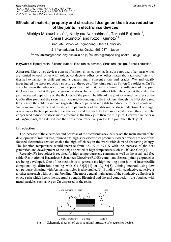
Electronics devices consist of silicon chips, copper leads, substrates and other parts which are jointed to each other with solder, conductive adhesive or other materials. Each coefficient of thermal expansion is different and it causes strain concentrations and cracks. We analytically investigated the stress reduction structure at the edge of the joints such as Sn-Ag-Cu solder or Cu/Sn alloy between the silicon chip and copper lead. At first, we examined the influence of the joint thickness and fillet at the joint edge on the stress. In the joint without fillet, the stress at the end of the joint increased depending on the thickness of the joint. The fillet of the joint increased the stress of the Cu/Sn alloy joint and the stress was increased depending on the thickness, though the fillet decreased the stress of the solder joint. We suggested the copper lead with slits to reduce the force of constraint. We compared the effects of the structure parameters of the slits on the stress reduction. The height was a more effective parameter than the width and the pitch. In the case of solder joint, the slits of the copper lead reduce the stress more effective in the thick joint than the thin joint. However, in the case of Cu3Sn joints, the slits reduced the stress more effectively in the thin joint than thick joint.

You might also be interested in these eBooks

Info:

Periodical:

Materials Science Forum (Volumes 783-786)

Pages:

2765-2770

Citation:

Online since:

May 2014

Export:

Price:

Permissions CCC:

Permissions PLS:

Сopyright:

© 2014 Trans Tech Publications Ltd. All Rights Reserved

Share:

Citation:

* - Corresponding Author

[1] C. M. Zetterling, L. Lanni, R. Ghandi, B. G. Malm, and M. Östling Future high temperature applications for SiC integrated circuits, Phys. Status Solidi C 9, No. 7, (2012) 1647-1650.

DOI: 10.1002/pssc.201100689

Google Scholar

[2] Karsten Guth, Dirk Siepe, Jens Görlich, Holger Torwesten, Roman Roth, Frank Hille and Frank Umbach, New assembly and interconnects beyond sintering methods, Power Conversion Intelligent Motion Europe 2010, Berlin (2010) 232-237.

Google Scholar

[3] T Fujimoto, S Fukumoto, T Miyazaki, Y Kashiba, K Shiotani and K Fujimoto, Bonding of copper to silicon chips using vapor-deposited tin film, Journal of Physics: Conference Series, Vol. 379 (2012) 1-7.

DOI: 10.1088/1742-6596/379/1/012026

Google Scholar

[4] J.F. Li, P.A. Agyakwa and C.M. Johnson, Interfacial reaction in Cu/Sn/Cu system during the transient liquid phase soldering process, Acta Materialia, Vol. 59, No. 3(2011)1198-1211.

DOI: 10.1016/j.actamat.2010.10.053

Google Scholar

[5] J.F. Li, P.A. Agyakwa and C.M. Johnson, Kinetics of Ag3Sn growth in Ag-Sn-Ag system during transient liquid phase soldering process, Acta Materialia, Vol. 58, No. 9(2010)3429-3443.

DOI: 10.1016/j.actamat.2010.02.018

Google Scholar

[6] A. Hirose, N. Takeda, H. Tatsumi, Y. Akada, T. Ogura, E. Ide and T. Morida, Low Temperature Sintering Bonding Process Using Ag Nanoparticles Derived from Ag2O for Packaging of High-temperature Electronics, Materials Science Forum, Vol. 706-709 (2012).

DOI: 10.4028/www.scientific.net/msf.706-709.2962

Google Scholar

[7] R.J. Fields and S.R. Low, Physical and Mechanical Properties of Intermetallic Compounds Commonly Found in Solder Joints, The Metal science of joining (1991) 165-174.

Google Scholar

[8] G. L Pearson, W. T Read Jr. and W. L Feldmann, Deformation and fracture of small silicon crystals, Acta Metallurgica, Vol. 5, No. 4 (1957) 181-191.

DOI: 10.1016/0001-6160(57)90164-5

Google Scholar

[9] X. Deng, N. Chawla, K.K. Chawla and M. Koopman, Deformation behavior of (Cu, Ag)-Sn intermetallics by nanoindentation, Acta Materialia, Vol. 52, No. 14 (2004) 4291-4303.

DOI: 10.1016/j.actamat.2004.05.046

Google Scholar

[10] S. Wakasugi, Y. Nishi, Y. Goto and T. Furukawa, Constitutive Relations between Stress, Strain-Rate and Temperature of Copper, Transactions of the Japan Society of Mechanical Engineers A Vol. 56, No. 530 (1990) 2152-2156.

DOI: 10.1299/kikaia.56.2152

Google Scholar

[11] K. Terasaki, K. Nagano, H. Miura and T. Nakatsuka, Evaluation of Thermal Fatigue Life of Pb-free Solder Joints for Use in Peripheral-lead-type LSI Packages, 7th Symposium on Microjoining and Assembly Technology in electronics, Vol. 7 (2001).

Google Scholar