p.978
p.982
p.986
p.990
p.995
p.999
p.1003
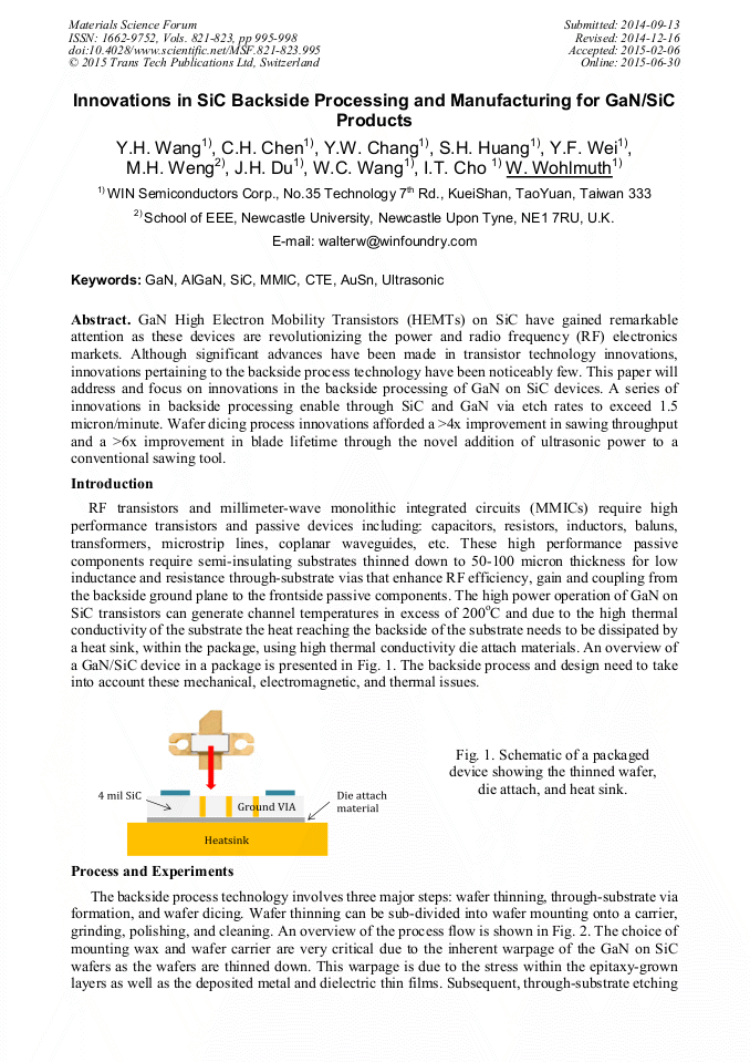
p.1007
p.1011
Innovations in SiC Backside Processing and Manufacturing for GaN/SiC Products

Abstract:
GaN High Electron Mobility Transistors (HEMTs) on SiC have gained remarkable attention as these devices are revolutionizing the power and radio frequency (RF) electronics markets. Although significant advances have been made in transistor technology innovations, innovations pertaining to the backside process technology have been noticeably few. This paper will address and focus on innovations in the backside processing of GaN on SiC devices. A series of innovations in backside processing enable through SiC and GaN via etch rates to exceed 1.5 micron/minute. Wafer dicing process innovations afforded a >4x improvement in sawing throughput and a >6x improvement in blade lifetime through the novel addition of ultrasonic power to a conventional sawing tool.

Info:
Periodical:
Pages:
995-998
Citation:
Online since:
June 2015
Price:
Сopyright:
© 2015 Trans Tech Publications Ltd. All Rights Reserved
Share:
Citation: