Field Emission Characteristics of AlN Coated Silicon Nanocone Arrays
p.797
p.797
Single-Crystal Uniform Tubes of ZnO
p.801
p.801
Synthesis and Optical Characterizations of ZnO Nanorods
p.805
p.805
New p-n Junction Photodetector Using Optimized ZnO Nanorod Array
p.809
p.809
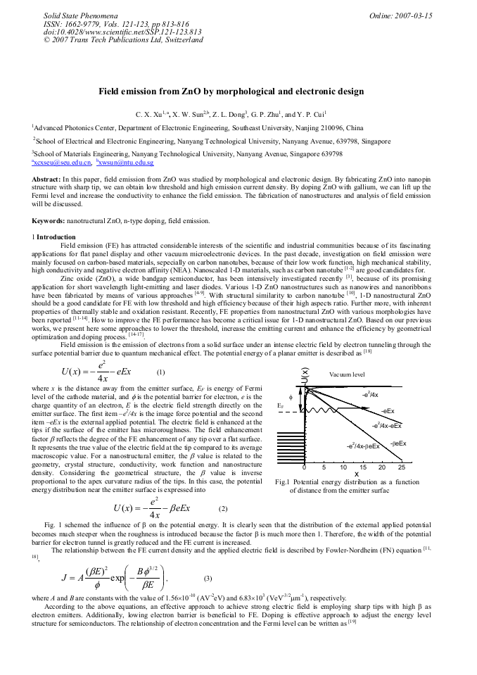
Field Emission from ZnO by Morphological and Electronic Design
p.813
p.813
Nano-Displacement Sensing and Estimation (nDSE): Enabling Technology for Nano Metrology and Fabrication
p.817
p.817
Six-DOF Nanomanipulation Tools for Nanoscale Device Prototyping and Fabrication
p.823
p.823
Imaging and Characterization of Self-Assembled Soft Nanostructures by Atomic Force Microscopy
p.829
p.829
Nanomeasure of Esaki Negative Resistance on p-Type GaAs(110) Surfaces
p.835
p.835
Field Emission from ZnO by Morphological and Electronic Design

Abstract:
In this paper, field emission from ZnO was studied by morphological and electronic design. By fabricating ZnO into nanopin structure with sharp tip, we can obtain low threshold and high emission current density. By doping ZnO with gallium, we can lift up the Fermi level and increase the conductivity to enhance the field emission. The fabrication of nanostructures and analysis of field emission will be discussed.
You might also be interested in these eBooks

Info:
Periodical:
Solid State Phenomena (Volumes 121-123)
Pages:
813-816
Citation:
Online since:
March 2007
Keywords:
Price:
Сopyright:
© 2007 Trans Tech Publications Ltd. All Rights Reserved
Share:
Citation: