p.101
p.105
p.109
p.113
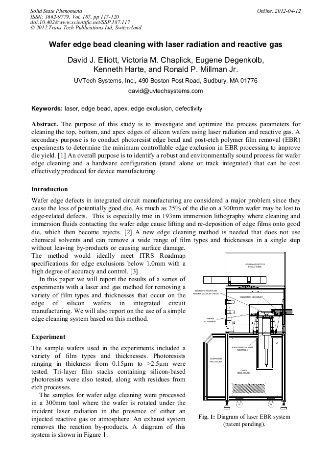
p.117
p.123
p.127
p.131
p.137
Wafer Edge Bead Cleaning with Laser Radiation and Reactive Gas

Abstract:
The purpose of this study is to investigate and optimize the process parameters for cleaning the top, bottom, and apex edges of silicon wafers using laser radiation and reactive gas. A secondary purpose is to conduct photoresist edge bead and post-etch polymer film removal (EBR) experiments to determine the minimum controllable edge exclusion in EBR processing to improve die yield. [ An overall purpose is to identify a robust and environmentally sound process for wafer edge cleaning and a hardware configuration (stand alone or track integrated) that can be cost effectively produced for device manufacturing.
Info:
Periodical:
Pages:
117-120
DOI:
Citation:
Online since:
April 2012
Keywords:
Price:
Сopyright:
© 2012 Trans Tech Publications Ltd. All Rights Reserved
Share:
Citation: