p.136
p.139
p.143
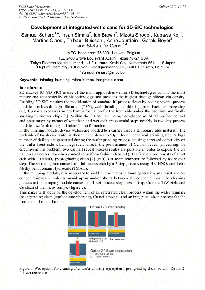
p.146
p.150
p.154
p.161
p.165
p.169
Development of Integrated Wet Cleans for 3D-SIC Technologies

Abstract:
3D stacked IC (3D-SIC) is one of the main approaches within 3D technologies as it is the most mature and economically viable technology and provides the highest through silicon via density. Enabling 3D SIC requires the modification of standard IC process flows by adding several process modules, such as through silicon via (TSV), wafer bonding and thinning, prior backside processing (e.g. Cu nails exposure), micro bumps formation for the front side and/or the backside and finally stacking to another chips [. Within the 3D-SIC technology developed at IMEC, surface control and preparation by means of wet clean and wet etch are essential steps notably in two key process modules: wafer thinning and micro bump formation.
Info:
Periodical:
Pages:
150-153
DOI:
Citation:
Online since:
December 2012
Keywords:
Price:
Сopyright:
© 2013 Trans Tech Publications Ltd. All Rights Reserved
Share:
Citation: