Watermark Formation on Bare Silicon: Impact of Illumination and Substrate Doping
p.89
p.89
Selective Nitride Etching with Phosphoric and Sulfuric Acid Mixtures Using a Single-Wafer Wet Processor
p.93
p.93
Single Wafer Selective Silicon Nitride Removal with Phosphoric Acid and Steam
p.97
p.97
Pt Etching Method at Low Temperature Using Electrolyzed Sulfuric Acid Solution
p.101
p.101
Nickel Selective Etch for Contacts on Ge Based Devices
p.105
p.105
Study of Wetting of Nanostructures Using Decoration by Etching
p.111
p.111
Impact of Electrostatic Effects on Wet Etching Phenomenon in Nanoscale Region
p.115
p.115
Freeze Drying of High Aspect Ratio Structures
p.119
p.119
Effect of DI-Water Dilution and Etchant Arm Movement on Spinning Type Wet Etch
p.125
p.125
Nickel Selective Etch for Contacts on Ge Based Devices

Abstract:
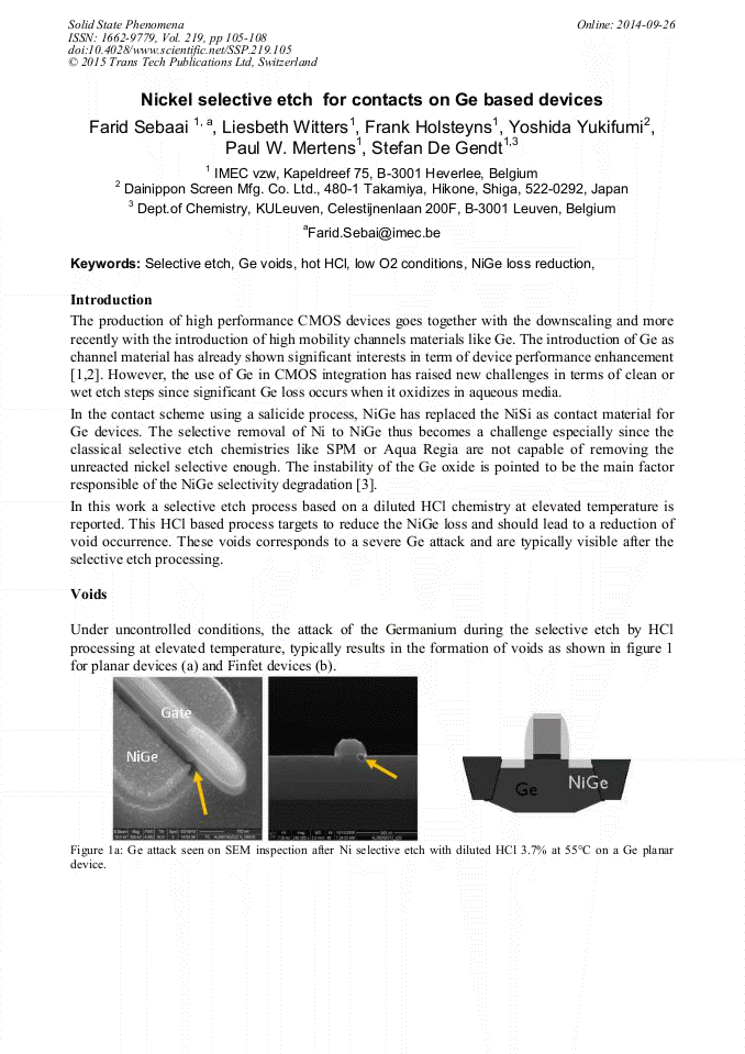
of high mobility channels materials like Ge. The introduction of Ge as channel material has already shown significant interests in term of device performance enhancement [1,2]. However, the use of Ge in CMOS integration has raised new challenges in terms of clean or wet etch steps since significant Ge loss occurs when it oxidizes in aqueous media.
You might also be interested in these eBooks
Info:
Periodical:
Solid State Phenomena (Volume 219)
Pages:
105-108
DOI:
Citation:
Online since:
September 2014
Keywords:
Price:
Сopyright:
© 2015 Trans Tech Publications Ltd. All Rights Reserved
Share:
Citation: