p.183
p.187
p.193
p.197
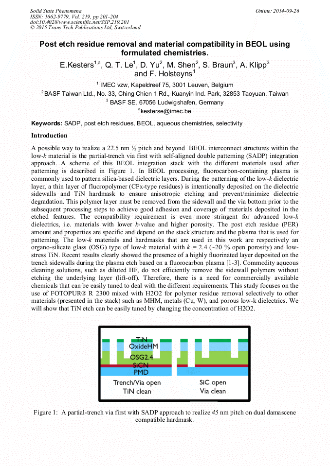
p.201
p.205
p.209
p.213
p.217
Post Etch Residue Removal and Material Compatibility in BEOL Using Formulated Chemistries

Abstract:
A possible way to realize a 22.5 nm 1⁄2 pitch and beyond BEOL interconnect structures within the low-k material is the partial-trench via first with self-aligned double patterning (SADP) integration approach. A scheme of this BEOL integration stack with the different materials used after patterning is described in Figure 1. In BEOL processing, fluorocarbon-containing plasma is commonly used to pattern silica-based dielectric layers. During the patterning of the low-k dielectric layer, a thin layer of fluoropolymer (CFx-type residues) is intentionally deposited on the dielectric sidewalls and TiN hardmask to ensure anisotropic etching and prevent/minimize dielectric degradation. This polymer layer must be removed from the sidewall and the via bottom prior to the subsequent processing steps to achieve good adhesion and coverage of materials deposited in the etched features. The compatibility requirement is even more stringent for advanced low-k dielectrics, i.e. materials with lower k-value and higher porosity. The post etch residue (PER) amount and properties are specific and depend on the stack structure and the plasma that is used for patterning. The low-k materials and hardmasks that are used in this work are respectively an organo-silicate glass (OSG) type of low-k material with k = 2.4 (~20 % open porosity) and low-stress TiN. Recent results clearly showed the presence of a highly fluorinated layer deposited on the trench sidewalls during the plasma etch based on a fluorocarbon plasma [1-3]. Commodity aqueous cleaning solutions, such as diluted HF, do not efficiently remove the sidewall polymers without etching the underlying layer (lift-off). Therefore, there is a need for commercially available chemicals that can be easily tuned to deal with the different requirements. This study focuses on the use of FOTOPUR® R 2300 mixed with H2O2 for polymer residue removal selectively to other materials (presented in the stack) such as MHM, metals (Cu, W), and porous low-k dielectrics. We will show that TiN etch can be easily tuned by changing the concentration of H2O2.
Info:
Periodical:
Pages:
201-204
DOI:
Citation:
Online since:
September 2014
Authors:
Keywords:
Price:
Сopyright:
© 2015 Trans Tech Publications Ltd. All Rights Reserved
Share:
Citation: