p.86
p.89
p.92
p.95
p.98
p.101
p.105
p.108
p.111
Fabrication of Photonic Crystals by Holographic Lithography Method
Abstract:
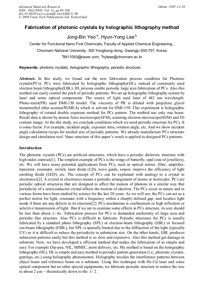
In this study, we found out the new fabrication process condition for Photonic crystals(PCs). PCs were fabricated by holographic lithography(HL), instead of commonly used electron beam lithography(EBL). HL process enable periodic large area fabrication of PCs. Also this method can easily control the pitch of periodic patterns. We set up holographic lithography system by laser and some optical components. The source of light used laser of 442 nm wavelength. Photo-resist(PR) used DMI-150 model. The viscosity of PR is diluted with propylene glycol monomethyl ether acetate(PGMEA) which is solvent for DMI-150. This experiment is holographic lithography of rotated double exposure method for PCs pattern. The method use only one beam. Result data is shown by atomic force microscope(AFM), scanning electron microscope(SEM) and 3D contour image. At the this study, we conclude conditions which we need periodic structure for PCs. It is some factor. For example, incident angle, exposure time, rotation angle, etc. And we show incident angle calculation recipe for needed size of periodic patterns. We already manufacture PCs structure design and simulation tool. Nano structure of this paper’s result is applied to designed PCs patterns.
Info:
Periodical:
Pages:
98-100
DOI:
Citation:
Online since:
November 2007
Authors:
Price:
Сopyright:
© 2008 Trans Tech Publications Ltd. All Rights Reserved
Share:
Citation:


