p.40
p.48
p.54
p.61
p.69
p.75
p.81
p.90
p.94
Toward Sub-20 nm Magnetic Tunnel Junction for Embedded Cache Memory

Abstract:
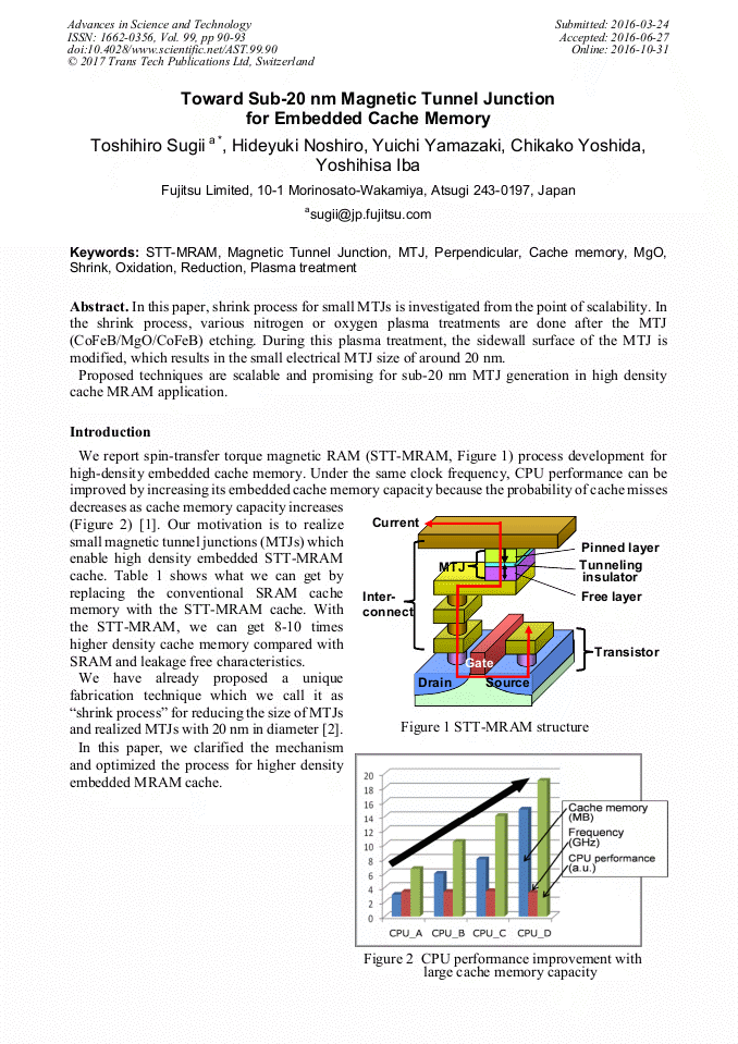
In this paper, shrink process for small MTJs is investigated from the point of scalability. In the shrink process, various nitrogen or oxygen plasma treatments are done after the MTJ (CoFeB/MgO/CoFeB) etching. During this plasma treatment, the sidewall surface of the MTJ is modified, which results in the small electrical MTJ size of around 20 nm.Proposed techniques are scalable and promising for sub-20 nm MTJ generation in high density cache MRAM application.
Info:
Periodical:
Pages:
90-93
DOI:
Citation:
Online since:
October 2016
Keywords:
Price:
Сopyright:
© 2017 Trans Tech Publications Ltd. All Rights Reserved
Share:
Citation: