A Study on Laser Cleaning of Al2O3 Grinding Wheels
p.359
p.359
Comparison of Laser Cleaning of Al2O3 and CBN Grinding Wheels
p.365
p.365
A Study of the Characteristics of the Diamond Dresser in the CMP Process
p.371
p.371
A Study on the Dressing Rate in CMP Pad Conditioning
p.377
p.377
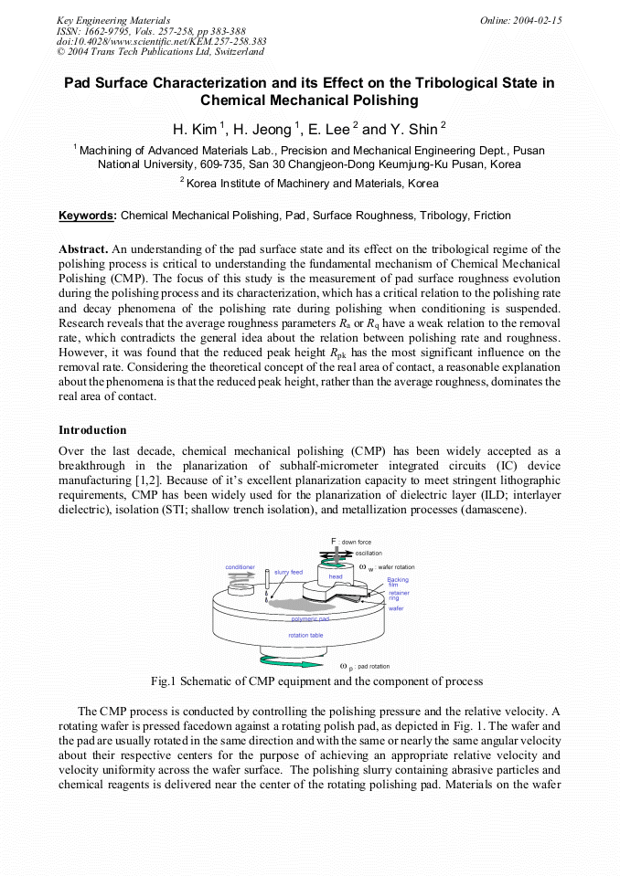
Pad Surface Characterization and its Effect on the Tribological State in Chemical Mechanical Polishing
p.383
p.383
Chemical and Mechanical Characterizations of the Passivation Layer of Copper in Organic Acid Based Slurries and its CMP Performance
p.389
p.389
A Study of an Ultra-Precision CNC Polishing System
p.395
p.395
Pressure-Based Grinding and Polishing of Free-Form Lenses with Spherical Tools
p.401
p.401
Effect of Pre-Thin-Surface Grinding on Copper Chemical Mechanical Polishing
p.407
p.407
Pad Surface Characterization and its Effect on the Tribological State in Chemical Mechanical Polishing

Abstract:
You might also be interested in these eBooks
Info:
Periodical:
Key Engineering Materials (Volumes 257-258)
Pages:
383-388
Citation:
Online since:
February 2004
Authors:
Price:
Сopyright:
© 2004 Trans Tech Publications Ltd. All Rights Reserved
Share:
Citation: