p.247
p.251
p.257
p.261
p.265
p.269
p.273
p.277
p.281
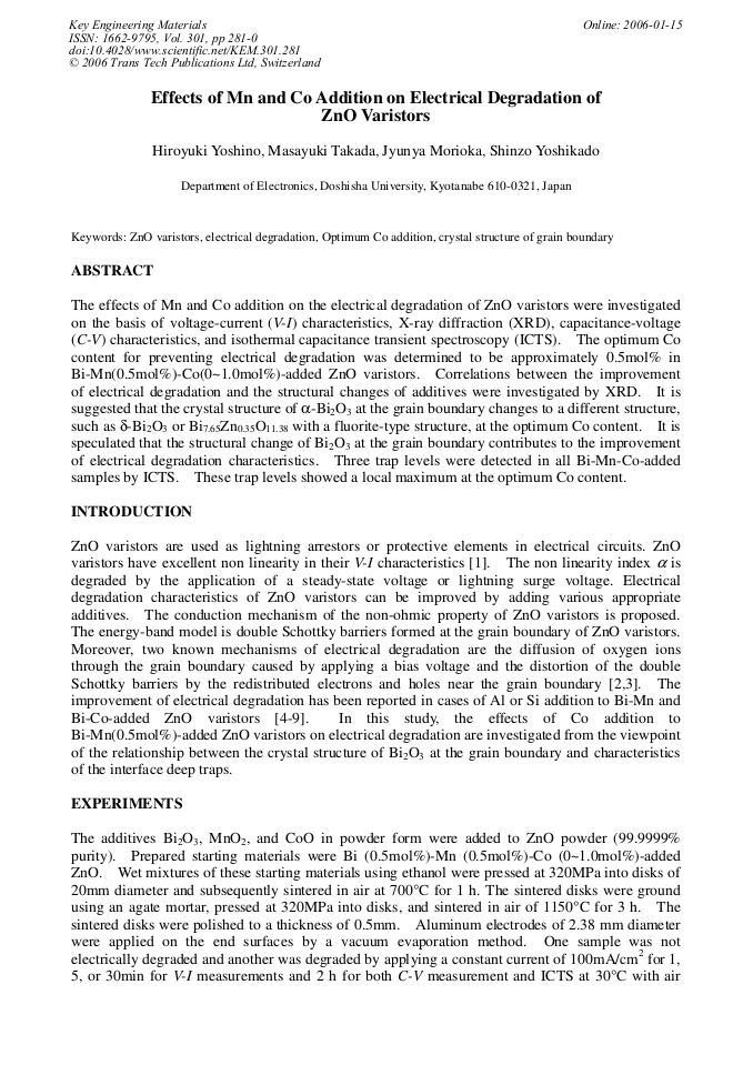
Effect of Mn and Co Addition on Electrical Degradation of ZnO Varistors
Abstract:
The effects of Mn and Co addition on the electrical degradation of ZnO varistors were investigated on the basis of voltage-current (V-I) characteristics, X-ray diffraction (XRD), capacitance-voltage (C-V) characteristics, and isothermal capacitance transient spectroscopy (ICTS). The optimum Co content for preventing electrical degradation was determined to be approximately 0.5mol% in Bi-Mn(0.5mol%)-Co(0~1.0mol%)-added ZnO varistors. Correlations between the improvement of electrical degradation and the structural changes of additives were investigated by XRD. It is suggested that the crystal structure of a-Bi2O3 at the grain boundary changes to a different structure, such as d-Bi2O3 or Bi7.65Zn0.35O11.38 with a fluorite-type structure, at the optimum Co content. It is speculated that the structural change of Bi2O3 at the grain boundary contributes to the improvement of electrical degradation characteristics. Three trap levels were detected in all Bi-Mn-Co-added samples by ICTS. These trap levels showed a local maximum at the optimum Co content.
Info:
Periodical:
Pages:
281-0
DOI:
Citation:
Online since:
January 2006
Price:
Сopyright:
© 2006 Trans Tech Publications Ltd. All Rights Reserved
Share:
Citation:


