Effects of Pretreatments on Deposition Rate of Films in Aerosol Deposition Method

Article Preview

Abstract:

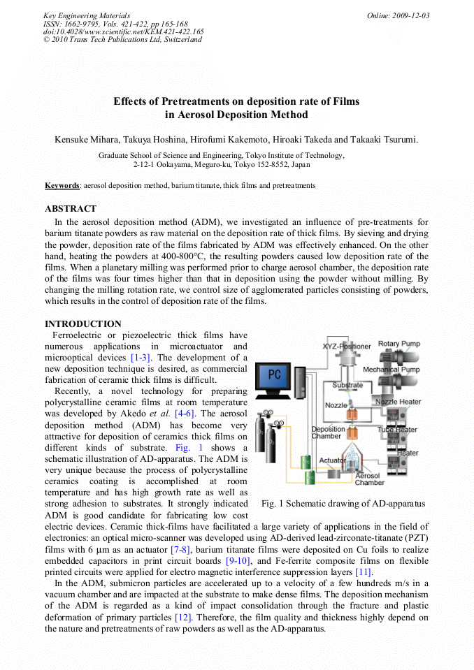
In the aerosol deposition method (ADM), we investigated an influence of pre-treatments for barium titanate powders as raw material on the deposition rate of thick films. By sieving and drying the powder, deposition rate of the films fabricated by ADM was effectively enhanced. On the other hand, heating the powders at 400-800°C, the resulting powders caused low deposition rate of the films. When a planetary milling was performed prior to charge aerosol chamber, the deposition rate of the films was four times higher than that in deposition using the powder without milling. By changing the milling rotation rate, we control size of agglomerated particles consisting of powders, which results in the control of deposition rate of the films.

You might also be interested in these eBooks

Info:

Periodical:

Key Engineering Materials (Volumes 421-422)

Pages:

165-168

Citation:

Online since:

December 2009

Export:

Price:

Permissions CCC:

Permissions PLS:

Сopyright:

© 2010 Trans Tech Publications Ltd. All Rights Reserved

Share:

Citation:

[1] M. Sayer and K. Sreenivas: Science 247 (1990) 1056.

Google Scholar

[2] J. Akedo and M. Lebedev: Recent Res. Devel. Mat. Sci. 2, Research Signpost, India, (2001).

Google Scholar

[3] I. R. Abothu, Y. Ito, P. Poosanaans, S. kalpat, S. Komarneni and K. Uchino: Ferroelectrics 232 (1999) 191.

DOI: 10.1080/00150199908015791

Google Scholar

[4] J. Akedo et al : Sens. Actuat. A, vol. 69 pp.106-112, (1998).

Google Scholar

[5] J. Akedo et al : Jpn. J. Appl. Phys. Vol. 38 pp.5397-5401, (1999).

Google Scholar

[6] J. Akedo et al : Appl. Phys. Lett. vol. 77 pp.1710-1712, (2000).

Google Scholar

[7] N. Asai, R. Matsuda, M. Watanabe, H. Takayama, S. Yamada, A. Mase, M. Shikida, K. Sato, M. Lebedev, and J. Akedo, A novel High Resolution Optical Scanner Actuated by Aerosol Deposited PZT Films. Proc. of MEMS 2003, 2003, pp.247-250.

DOI: 10.1109/memsys.2003.1189732

Google Scholar

[8] J. Akedo, M. Lebedev, H. Sato, and J. H. Park, Jpn. J. Appl. Phys., 2005, 44, pp.7072-7077.

Google Scholar

[9] Y. Imanaka and J. Akedo, Proceedings of the 54th Electronic Components and Technology Conference(ECTC), 2004, pp.1614-1620.

Google Scholar

[10] S. -M. Nam, H. Yabe, H. Kakemoto, S. Wada, T. Tsurumi, and J. Akedo, Trans MRS Jpn., 2004, 29(4), pp.1215-1218.

Google Scholar

[11] S. Sugimoto K. Haga, M. Nakada, T. Kagotani, K. Inomata, and J. Akedo, I"TERMAG 2005, 2005, Nagoya, Japan, April 4-8, EC-04.

Google Scholar

[12] Jun Akedo, J. Am. Ceram. Soc., 89.

Google Scholar

[6] 1834-1839 (2006).

Google Scholar

[13] H. Adachi, Y. Kuroda, T. Imahashi and K. Yanagisawa: Jpn J. Appl. Phys. 36 (1997) 1159.

Google Scholar

[14] C. Hayashi, S. Kashu, M. Oda and F. Naruse: Mater. Sci. Eng. A 163 (1993) 157.

Google Scholar

[15] Jun Akedo, Maxim LEBEDEV ; Jpn. J. Appl. Phys, Vol. 41 (2002) pp.6980-6984.

Google Scholar

[16] J. Akedo and M. Lebedev ; Jpn. J. Appl. Phys., 40, 5528 (2001).

Google Scholar

[17] J. Akedo ; Material Science Form, 449, 43 (2004) E-mail: mihara. k. aa@m. titech. ac. jp Fax Number: +81-3-5734-2514.

Google Scholar