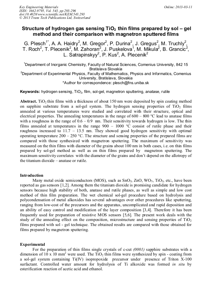
Structure of Hydrogen Gas Sensing TiO2 Thin Films Prepared by Sol-Gel Method and their Comparison with Magnetron Sputtered Films

Article Preview

Abstract:

TiO2 thin films with a thickness of about 150 nm were deposited by spin coating method on sapphire substrate from a sol-gel system. The hydrogen sensing properties of TiO2 films annealed at various temperatures were studied and correlated with their structure, optical and electrical properties. The annealing temperatures in the range of 600 800 °C lead to anatase films with a roughness in the range of 0.6 0.9 nm. Their sensitivity towards hydrogen is low. The thin films annealed at temperatures in the range 900 1000 °C consist of rutile phase and their roughness increased to 11.7 13.5 nm. They showed good hydrogen sensitivity with optimal operating temperature 200 250 °C. The structure and sensing properties of the prepared films are compared with those synthesized with magnetron sputtering. The maximum of sensitivity was measured on the thin films with diameter of the grains about 100 nm in both cases, i.e. on thin films prepared by sol-gel method as well as on thin films prepared by magnetron sputtering. The maximum sensitivity correlates with the diameter of the grains and dont depend on the allotropy of the titanium dioxide anatase or rutile.

You might also be interested in these eBooks

Info:

Periodical:

Pages:

293-296

Citation:

Online since:

March 2013

Export:

Price:

Permissions CCC:

Permissions PLS:

Сopyright:

© 2013 Trans Tech Publications Ltd. All Rights Reserved

Share:

Citation:

[1] S. M. Kanan, O. M. El-Kadri, I. A. Abu-Yousef , M. C. Kanan: Sensors Vol. 9 (2009), p.8158.

DOI: 10.3390/s91008158

Google Scholar

[2] C. Wang, L. Yin, L. Zhang, D. Xiang, R. Gao: Sensors Vol. 10 (2010), p. (2088).

Google Scholar

[3] M. Epifani, A. Helwig, J. Arbiol, R. Diaz, L. Francioso, P. Siciliano, G. Mueller, J. R. Morante: Sensors and Actuators B Vol. 130 (2008), p.599.

DOI: 10.1016/j.snb.2007.10.016

Google Scholar

[4] D. Mardare, N. Iftimie, M. Crişan, M. Raileanu, A. Yildiz, T. Coman, K. Pomoni, A. Vomvas: J. Non Cryst. Solids Vol. 357 (2011), p.1774.

DOI: 10.1016/j.jnoncrysol.2011.01.035

Google Scholar

[5] D.S. Presicce, L. Francioso, M. Epifani, P. Siciliano, A. Ficarella: Sensors and Actuators B Vol. 111–112 (2005), p.52.

DOI: 10.1016/j.snb.2005.07.050

Google Scholar

[6] F. Hossein-Babaei, M. Keshmiri, M. Kakavand, T. Troczynski: Sensors and Actuators B Vol. 110 (2005).

DOI: 10.1016/j.snb.2005.01.010

Google Scholar

[7] A. Haidry, M. Vargová, P. Ďurina, J. Greguš, M. Truchly, T. Roch, T. Plecenik, M. Zahoran, J. Puškelová, P. Kuš, A. Plecenik, G. Plesch: Applied Surface Science Vol. 259 (2012), p.270.

DOI: 10.1016/j.apsusc.2012.07.030

Google Scholar

[8] Huber, A. Brodyanski, M. Scheib, A. Orendorz, C. Ziegler, H. Gnaser: Thin Solid Films Vol. 472 (2005), p.114.

DOI: 10.1016/j.tsf.2004.06.120

Google Scholar

[9] A. Al-Homoudi, J.S. Thakurb, R. Naik, G.W. Auner, G. Newaz, Applied Surface Science Vol. 253 (2007) p.8607.

DOI: 10.1016/j.apsusc.2007.04.068

Google Scholar

[10] T. Roch, E. Dobrocka, M. Mikula, A. Pidik, P. Durina, A.A. Haidry, T. Plecenik, M. Truchly, B. Grancic, A. Plecenik, P. Kus, Journal of Crystal Growth Vol. 338 (2012) p.118.

DOI: 10.5162/imcs2012/p2.0.5

Google Scholar