p.1089
p.1093
p.1098
p.1103
p.1107
p.1111
p.1115
p.1119
p.1123
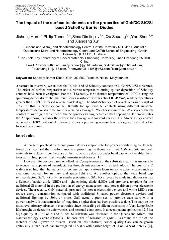
The Impact of the Surface Treatments on the Properties of Gan/3C-SiC/Si Based Schottky Barrier Diodes
Abstract:
In this work, we studied the effect of surface preparation and substrate temperature during sputter deposition of Schottky contacts on N-GaN/SiC/Si substrates, looking at parameters such as on-resistance, reverse leakage, and contact barrier height. Ti, Ni and Mo were sputtered to form the contacts, and we characterized the I-V curves with the different substrate temperatures during the sputtering as shown in Figure 1. For the Ti Schottky contact, the substrate temperature of 100oC during the sputtering demonstrates the minimum series resistance with Rs about 0.04cm2, while temperatures greater than 3000C increased reverse bias leakage. The Mott-Schottky plot reveals a barrier height of 1.2V for this contact. Results for sputtered Ni contacts using different substrate temperatures will also be presented, as well as the effect of Ar sputter cleaning before contact deposition.
Info:
Periodical:
Pages:
1111-1114
Citation:
Online since:
January 2013
Authors:
Keywords:
Price:
Сopyright:
© 2013 Trans Tech Publications Ltd. All Rights Reserved
Share:
Citation:


