High-Speed Dicing of SiC Wafers by Femtosecond Pulsed Laser

Article Preview

Abstract:

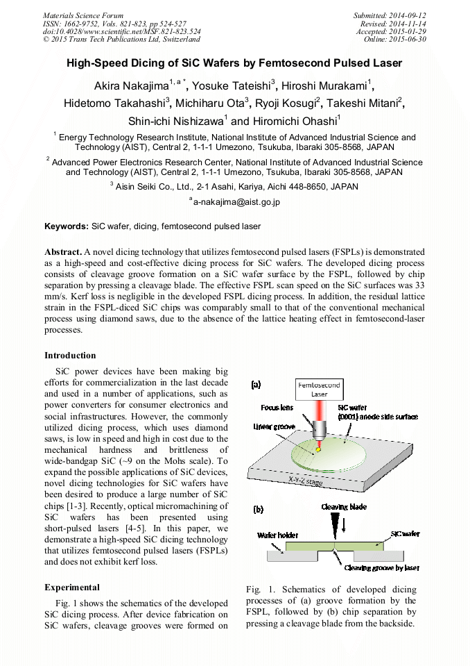
A novel dicing technology that utilizes femtosecond pulsed lasers (FSPLs) are demonstrated as a high-speed and cost-effective dicing process for SiC wafers. The developed dicing process consists of cleavage groove formation on a SiC wafer surface by the FSPL, followed by chip separation by pressing a cleavage blade. The effective FSPL scan speed on the SiC surfaces was 33 mm/s. Kerf loss can be negligible in the developed FSPL dicing process. In addition, the residual lattice strain in the FSPL-diced SiC chips was comparably small to that of the conventional mechanical process using diamond saws, due to the absence of the lattice heating effect in femtosecond-laser processes.

You might also be interested in these eBooks

Info:

Periodical:

Materials Science Forum (Volumes 821-823)

Pages:

524-527

Citation:

Online since:

June 2015

Export:

Price:

Permissions CCC:

Permissions PLS:

Сopyright:

© 2015 Trans Tech Publications Ltd. All Rights Reserved

Share:

Citation:

* - Corresponding Author

[1] D. Lewke, M. Koitzsch, M. Schellenberger, L. Pfitzner, H. Ryssel, H. Zühlke, Proc. Mater. Res. Soc. Symp. Vol. 1433 (2012) p.25.

DOI: 10.1557/opl.2012.1035

Google Scholar

[2] S. Green, D. Perrottet and B. Richerzhagen, Proc. IEEE/SEMI Advanced Semiconductor Manufacturing Conference and Workshop (2006), p.166.

Google Scholar

[3] Y. Sano, H. Nishikawa, Y. Okada, K. Yamamura, S. Matsuyama, K. Yamauchi, Mater. Sci. Forum Vol. 778–780 (2013), p.759.

Google Scholar

[4] Y. Dong, R. Nair, R. Molian and P. Molian, J. Micromech. Microeng. Vol. 18 (1992), p.035022 (2008).

DOI: 10.1088/0960-1317/18/3/035022

Google Scholar

[5] P. Molian, B. Pecholt, and S. Gupta, Appl. Surf. Science Vol. 255 (2009), p.4515.

Google Scholar

[6] R. Rupp, R. Gerlach, U. Kirchner, A. Schlӧgl, and R Kern, Mater. Sci. Forum Vol. 717–720 (2012), p.921.

Google Scholar