p.443
p.449
p.455
p.461
p.467
p.473
p.479
p.485
p.491
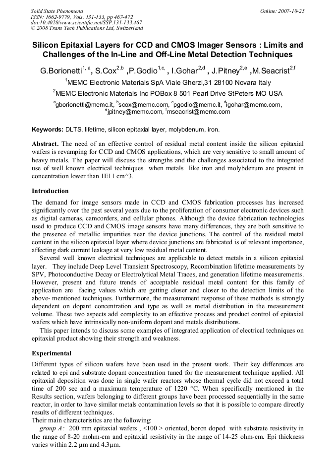
Silicon Epitaxial Layers for CCD and CMOS Imager Sensors : Limits and Challenges of the In-Line and Off-Line Metal Detection Techniques
Abstract:
The need of an effective control of residual metal content inside the silicon epitaxial wafers is revamping for CCD and CMOS applications, which are very sensitive to small amount of heavy metals. The paper will discuss the strengths and the challenges associated to the integrated use of well known electrical techniques when metals like iron and molybdenum are present in concentration lower than 1E11 cm^3.
Info:
Periodical:
Pages:
467-472
Citation:
Online since:
October 2007
Authors:
Keywords:
Price:
Сopyright:
© 2008 Trans Tech Publications Ltd. All Rights Reserved
Share:
Citation:


