Observation of Leakage Sites in High-k Gate Dielectrics in MOSFET Devices by Electron-Beam-Induced Current Technique

Article Preview

Abstract:

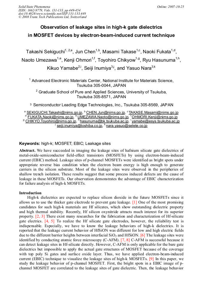
We have succeeded in imaging the leakage sites of hafnium silicate gate dielectrics of metal-oxide-semiconductor field-effect transistors (MOSFETs) by using electron-beam-induced current (EBIC) method. Leakage sites of p-channel MOSFETs were identified as bright spots under appropriate reverse bias condition when the electron beam energy is high enough to generate carriers in the silicon substrate. Most of the leakage sites were observed in the peripheries of shallow trench isolation. These results suggest that some process induced defects are the cause of leakage in these MOSFETs. Our observation demonstrates the advantage of EBIC characterization for failure analysis of high-k MOSFETs.

You might also be interested in these eBooks

Info:

Periodical:

Solid State Phenomena (Volumes 131-133)

Pages:

449-454

Citation:

Online since:

October 2007

Export:

Price:

Permissions CCC:

Permissions PLS:

Сopyright:

© 2008 Trans Tech Publications Ltd. All Rights Reserved

Share:

Citation:

[1] G. D. Wilk, R. M. Wallace, and J. M. Anthony, J. Appl. Phys. 89 (2001), p.5243.

Google Scholar

[2] M. R. Visokay, J. J. Chambers, A. L. Rotondaro, A. Shanware, and L. Colombo, Appl. Phys. Lett. 80 (2002), p.3183.

DOI: 10.1063/1.1476397

Google Scholar

[3] M. Koike, T. Ino, Y. Kammuta, M. Koyama, Y. Kamata, M. Suziki, Y. Mitani, and A. Nishiyama, Physical Review B 73 (2006) 125123.

Google Scholar

[4] H. Watanabe, M. Saitoh, N. Ikarashi, and T. Tatsumi, Appl. Phys. Lett. 85 (2004), p.449.

Google Scholar

[5] A. Callegari, E. Cartier, M. Gribelyuk, H.F. Okorn-Schmidt, and T. Zabel, J. Appl. Phys. 90 (2001), p.6466.

Google Scholar

[6] M. Terai, Y. Yabe, S. Fujieda, A. Morioka, S. Kotsuji, T. Iwamoto, M. Saitoh, T. Ogura, Y. Saito, and H. Watanabe, Jpn. J. Appl. Phys. 44 (2005) p.2441.

DOI: 10.1143/jjap.44.2441

Google Scholar

[7] K. Kyuno, K. Kita, and A. Toriumi, Appl. Phys. Lett. 86 (2005), 063510.

Google Scholar

[8] H. Watanabe, S. Kamiyama, N. Umezawa, K. Shiraishi, S. Yoshida, Y. Watanabe, T. Arikado, T. Chikyow, K. Yamada, and K. Yasutake, Jpn. J. Appl. Phys. 44 (2005), L1333.

DOI: 10.1143/jjap.44.l1333

Google Scholar

[9] J. Chen, T. Sekiguchi, N. Fukata, M. Takase, T. Chikyow, K. Yamabe, R. Hasunuma, Y. Akasaka, S. Inumiya, Y. Nara, and K. Yamada, Appl. Phys. Lett. 89 (2006) 222104.

DOI: 10.1063/1.2392988

Google Scholar

[10] S. Kamiyama, T. Miura, Y. Nara, and T. Arikado, Appl. Phys. Lett. 86 (2005) 222904.

Google Scholar

[11] T. Sekiguchi and K. Sumino: Rev. Sci. Instrum. 66 (1995), p.4277.

Google Scholar

[12] H.R. Kirk, Z. Radzimski, A. Romanovski, and G.A. Rozgonyi, J. Electrochem. Soc., 146 (1999) p.1529.

Google Scholar