Characterization of Low-k Dielectric Etch Residue on the Sidewall by Chemical Force Microscope
p.197
p.197
Optimized Wetting Behavior of Water-Based Cleaning Solutions for Plasma Etch Residue Removal by Application of Surfactants
p.201
p.201
Modification of Post-Etch Residues by UV for Wet Removal
p.207
p.207
"Damage Free" Cleaning for Advanced BEOL Interconnections
p.211
p.211
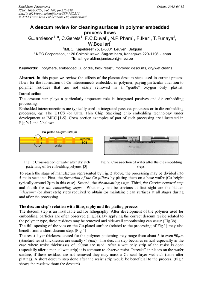
A Descum Review for Cleaning Surfaces in Polymer Embedded Process Flows
p.215
p.215
Influence of Photoresist and BARC Selection on the Efficiency of a Post-Etch Wet Strip in BEOL Applications
p.219
p.219
ESH Friendly Solvent for Stripping Positive and Negative Photoresists in 3D-Wafer Level Packaging and 3D-Stacked IC Applications
p.223
p.223
Tungsten Oxidation Kinetic after Wet Cleaning: XPS and ToF-SIMS Characterization
p.227
p.227
A Comparison between BTA and Amidoximes and their Interactions with Copper Surfaces
p.231
p.231
A Descum Review for Cleaning Surfaces in Polymer Embedded Process Flows

Abstract:
In this paper we review the effects of the plasma descum steps used in current process flows for the fabrication of Cu interconnects embedded in polymer, paying particular attention to polymer residues that are not easily removed in a gentle oxygen only plasma.
You might also be interested in these eBooks
Info:
Periodical:
Solid State Phenomena (Volume 187)
Pages:
215-218
DOI:
Citation:
Online since:
April 2012
Authors:
Keywords:
Price:
Сopyright:
© 2012 Trans Tech Publications Ltd. All Rights Reserved
Share:
Citation: