p.15
p.19
p.23
p.27
p.33
p.37
p.41
p.45
p.49
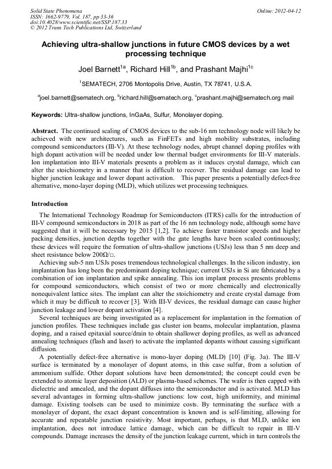
Achieving Ultra-Shallow Junctions in Future CMOS Devices by a Wet Processing Technique
Abstract:
The continued scaling of CMOS devices to the sub-16 nm technology node will likely be achieved with new architectures, such as FinFETs and high mobility substrates, including compound semiconductors (III-V). At these technology nodes, abrupt channel doping profiles with high dopant activation will be needed under low thermal budget environments for III-V materials. Ion implantation into III-V materials presents a problem as it induces crystal damage, which can alter the stoichiometry in a manner that is difficult to recover. The residual damage can lead to higher junction leakage and lower dopant activation. This paper presents a potentially defect-free alternative, mono-layer doping (MLD), which utilizes wet processing techniques.
Info:
Periodical:
Pages:
33-36
DOI:
Citation:
Online since:
April 2012
Authors:
Keywords:
Price:
Сopyright:
© 2012 Trans Tech Publications Ltd. All Rights Reserved
Share:
Citation:


