Large Area SiC Epitaxial Layer Growth in a Warm-Wall Planetary VPE Reactor

Article Preview

Abstract:

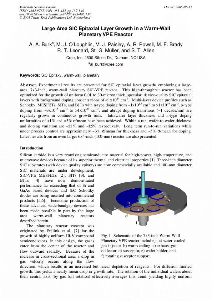
Experimental results are presented for SiC epitaxial layer growths employing a largearea, 7x3-inch, warm-wall planetary SiC-VPE reactor. This high-throughput reactor has been optimized for the growth of uniform 0.01 to 30-micron thick, specular, device-quality SiC epitaxial layers with background doping concentrations of <1x1014 cm-3. Multi-layer device profiles such as Schottky, MESFETs, SITs, and BJTs with n-type doping from ~1x1015 cm-3 to >1x1019 cm-3, p-type doping from ~3x1015 cm-3 to >1x1020 cm-3, and abrupt doping transitions (~1 decade/nm) are regularly grown in continuous growth runs. Intrawafer layer thickness and n-type doping uniformities of <1% and <5% s/mean have been achieved. Within a run, wafer-to-wafer thickness and doping variation are ~±1% and ~±5% respectively. Long term run-to-run variations while under process control are approximately ~3% s/mean for thickness and ~5% s/mean for doping. Latest results from an even larger 6x4-inch (100-mm) reactor are also presented.

You might also be interested in these eBooks

Info:

Periodical:

Materials Science Forum (Volumes 483-485)

Pages:

137-140

Citation:

Online since:

May 2005

Export:

Price:

Permissions CCC:

Permissions PLS:

Сopyright:

© 2005 Trans Tech Publications Ltd. All Rights Reserved

Share:

Citation:

[1] H. Morkoç, S. Strite, G. B. Gao, M. E. Lin, B. Sverdlov, and M. Burns, J. Appl. Phys., 76, 1363 (1994).

Google Scholar

[2] J. W. Milligan, S.T. Allen, J. J. Sumakeris, A. R. Powell, J. R. Jenny, and J. W. Palmour, GaAs MANTECH Conference Digest of Papers, Scottsdale, Az. (2003).

Google Scholar

[3] R. R. Siergiej, S. Sriram, R. C. Clarke, A. K. Agarwal, C. D. Brandt, A. A. Burk, Jr., T. J. Smith, A. Morse, and P. A. Orphanos, Tech. Digest Int. Conf. SiC and Rel. Mat'95, (Kyoto, Japan 1995), p.321.

DOI: 10.1109/drc.1995.496290

Google Scholar

[4] A. Agarwal, Sei-Hyung Ryu, C. Capell, J. Richmond, J. Palmour, H. Bartlow, P. Chow, S. Scozzie, W. Tipton, S. Baynes and K. Jones, Silicon Carbide and Related Materials 2003, Materials Science Forum Vols. 457-460 (2004) p.1141.

DOI: 10.4028/www.scientific.net/msf.457-460.1141

Google Scholar

[5] Cree, Inc. 4600 Silicon Drive, Durham NC, 27703.

Google Scholar

[6] M. Treu, R. Rupp, H. Brunner, F. Dahlquist and Ch. Hecht, Silicon Carbide and Related Materials 2003, Materials Science Forum Vols. 457-460 (2004) p.981.

DOI: 10.4028/www.scientific.net/msf.457-460.981

Google Scholar

[7] P. M. Frijlink, J. Crystal Growth, 93, 207 (1988).

Google Scholar

[8] P. M. Frijlink, J. L. Nicolas and P. Suchet, J. Crystal Growth, 107, 166 (1991).

Google Scholar

[9] Aixtron Inc. Kackerstr. 15-17, D-52072 Aachen, Germany.

Google Scholar

[10] R. Rupp, A. Wiedenhofer, D. Stephani, Mat. Sci. and Enginneering, B61-62 (1999), p.125.

Google Scholar

[11] A. A. Burk, Jr., M. J. O'Loughlin, and H. D. Nordby, Jr., J. Crystal Growth, Vol. 200 (1999), p.458.

Google Scholar

[12] M. J. O'Loughlin, H. D. Nordby, Jr., and A. A. Burk, Jr., Mat. Res. Soc. Symp. Proc. Vol 572 (1999), p.161.

Google Scholar

[13] B. Thomas, W. Bartsch, R. Stein, R. Schörner and D. Stephani, Silicon Carbide and Related Materials 2003, Materials Science Forum Vols. 457-460 (2004) p.181.

DOI: 10.4028/www.scientific.net/msf.457-460.181

Google Scholar

[14] T. Kimoto, A. Itoh, H. Akita, T. Urushidani, S. Jang, and H. Matsunami, Compound Semiconductors (1994), p.437. Fig. 5 RF Power map for 1 mm FETs sampled from a 3-inch wafer indicating 4 W/mm cw with >50% PAE at 3 GHz (VDS=50 V, IDQ=50 mA).

Google Scholar