p.305
p.319
p.325
p.333
p.341
p.355
p.375
p.387
p.403
RTP Requirements for CMOS Integration of Dual Work Function Phase Controlled Ni-FUSI (Fully Silicided) Gates with Simultaneous Silicidation of nMOS (NiSi) and pMOS (Ni-Rich Silicide) Gates on HfSiON

Abstract:
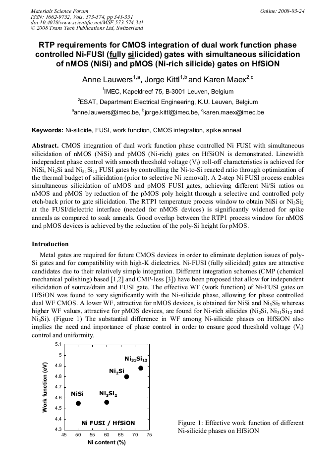
CMOS integration of dual work function phase controlled Ni FUSI with simultaneous silicidation of nMOS (NiSi) and pMOS (Ni-rich) gates on HfSiON is demonstrated. Linewidth independent phase control with smooth threshold voltage (Vt) roll-off characteristics is achieved for NiSi, Ni2Si and Ni31Si12 FUSI gates by controlling the Ni-to-Si reacted ratio through optimization of the thermal budget of silicidation (prior to selective Ni removal). A 2-step Ni FUSI process enables simultaneous silicidation of nMOS and pMOS FUSI gates, achieving different Ni/Si ratios on nMOS and pMOS by reduction of the pMOS poly height through a selective and controlled poly etch-back prior to gate silicidation. The RTP1 temperature process window to obtain NiSi or Ni3Si2 at the FUSI/dielectric interface (needed for nMOS devices) is significantly widened for spike anneals as compared to soak anneals. Good overlap between the RTP1 process window for nMOS and pMOS devices is achieved by the reduction of the poly-Si height for pMOS.
Info:
Periodical:
Pages:
341-351
Citation:
Online since:
March 2008
Authors:
Keywords:
Price:
Сopyright:
© 2008 Trans Tech Publications Ltd. All Rights Reserved
Share:
Citation: