p.1159
p.1163
p.1167
p.1171
p.1177
p.1183
p.1187
p.1191
p.1195
Discussion of Turn on Current Peaks of SiC Switches in Half Bridges

Abstract:
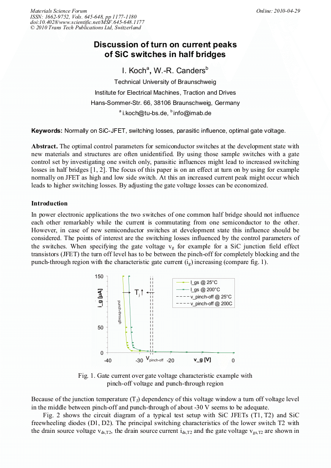
The optimal control parameters for semiconductor switches at the development state with new materials and structures are often unidentified. By using those sample switches with a gate control set by investigating one switch only, parasitic influences might lead to increased switching losses in half bridges [1, 2]. The focus of this paper is on an effect at turn on by using for example normally on JFET as high and low side switch. At this an increased current peak might occur which leads to higher switching losses. By adjusting the gate voltage losses can be economized.
Info:
Periodical:
Pages:
1177-1180
Citation:
Online since:
April 2010
Authors:
Keywords:
Price:
Сopyright:
© 2010 Trans Tech Publications Ltd. All Rights Reserved
Share:
Citation: