Change of the Characterization Techniques as Progress of CuInSe2-Based Thin-Film PV Technology

Article Preview

Abstract:

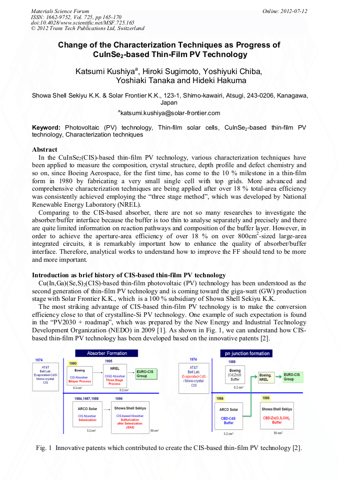
In the CuInSe2(CIS)-based thin-film PV technology, various characterization techniques have been applied to measure the composition, crystal structure, depth profile and defect chemistry and so on, since Boeing Aerospace, for the first time, has come to the 10 % milestone in a thin-film form in 1980 by fabricating a very small single cell with top grids. More advanced and comprehensive characterization techniques are being applied after over 18 % total-area efficiency was consistently achieved employing the “three stage method”, which was developed by National Renewable Energy Laboratory (NREL). Comparing to the CIS-based absorber, there are not so many researches to investigate the absorber/buffer interface because the buffer is too thin to analyse separately and precisely and there are quite limited information on reaction pathways and composition of the buffer layer. However, in order to achieve the aperture-area efficiency of over 18 % on over 800cm2-sized large-area integrated circuits, it is remarkably important how to enhance the quality of absorber/buffer interface. Therefore, analytical works to understand how to improve the FF should tend to be more and more important.

You might also be interested in these eBooks

Info:

Periodical:

Pages:

165-170

Citation:

Online since:

July 2012

Export:

Price:

Permissions CCC:

Permissions PLS:

Сopyright:

© 2012 Trans Tech Publications Ltd. All Rights Reserved

Share:

Citation:

[1] NEDO website [http://app3.infoc.nedo.go.jp/informations/koubo/kaiken/BE/nedopressorder. 2009-06-08.2039491773/]

Google Scholar

[2] Heisei 20 Report of Patent Trends of Solar Cells issued by Japan Patent Office in April, 2009.

Google Scholar

[3] R.A. Mickelsen and W.S. Chen, US Patent 4,335,266 (June 15, 1982).

Google Scholar

[4] K.M. Mitchell, C. Eberspacher, J.H. Ermer, K.L. Pauls, D.N. Pier, IEEE Trans. Electron. Devices (1990) pp.410-417.

DOI: 10.1109/16.46375

Google Scholar

[5] M.A. Green, K. Emery, Y. Hishikawa, W. Warta and E.D. Dunlop, Prog. Photovolt: Res. Appl. 19 (2011) pp.565-572.

DOI: 10.1002/pip.1150

Google Scholar

[6] D. Abou-Ras, R. Caballero, C.-H. Fischer, C.A. Kaufmann, I. Lauermann, R. Mainz, H. Mönig, A.Schöpke, C. Stephan, C. Streeck, S. Schorr, A. Eicke, M. Döbeli, B. Gade, J. Hinrichs, T. Nunney, H. Dijkstra, V. Hoffmann, D. Klemm, V. Efimova, A. Bergmaier, G. Dollinger, T. Wirth, W. Unger, A.A. Rockett, A. Perez-Rodriguez, J. Alvarez-Garcia, V. Izquierdo-Roca, T. Schmid, P.-P. Choi, M. Müller, F. Bertram, J. Christen, H. Khatri, R.W. Collins, S. Marsillac and I. Kötschau, Microsc. Microanal. (2011), pp.1-24

DOI: 10.1017/s1431927611000523

Google Scholar

[7] A.M. Gabor, J.R. Tuttle, D.S. Albin, M.A. Contreras, R. Noufi, A.M. Hermann, Appl. Phys. Lett., 65 (1994) pp.198-200.

Google Scholar

[8] Y. Tanaka, N. Akema, T. Morishita, D. Okumura, K. Kushiya, Proc. 17th ECPVSEC (2001) 989-994.

Google Scholar

[9] H.Sugimoto, T. Aramoto, Y.Kawaguchi, Y. Chiba, S. Kijima, Y. Fujiwara, Y. Tanaka, H. Hakuma, K. Kakegawa and K. Kushiya, Proc. 24th EUPVSEC (2009) 2465-2468.

DOI: 10.1557/proc-1165-m06-06

Google Scholar

[10] Y. Chiba, S. Kijima, H. Sugimoto, Y. Kawaguchi, M. Nagahashi, T. Morimoto, T. Yagioka, T. Miyano, T. Aramoto, Y. Tanaka, H. Hakuma, S. Kuriyagawa and K. Kushiya, 35th IEEE PVSC (2010) 164-168.

DOI: 10.1109/pvsc.2010.5616037

Google Scholar

[11] K. Kushiya, Y. Tanaka, H. Hakuma, S. Kijima, T. Aramoto, Y. Fujiwara, Y. Chiba, H. Sugimoto, Y. Kawaguchi, K. Kakegawa, Mater. Res. Soc. Symp. Proc. Volume 1165, 1165-M06-06, 2009.

DOI: 10.1557/proc-1165-m06-06

Google Scholar