p.825
p.829
p.833
p.837
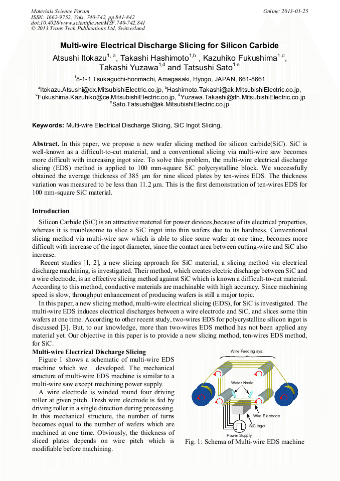
p.841
p.843
p.847
p.851
p.855
Multi-Wire Electrical Discharge Slicing for Silicon Carbide

Abstract:
In this paper, we propose a new wafer slicing method for silicon carbide(SiC). SiC is well-known as a difficult-to-cut material, and a conventional slicing via multi-wire saw becomes more difficult with increasing ingot size. To solve this problem, the multi-wire electrical discharge slicing (EDS) method is applied to 100 mm-square SiC polycrystalline block. We successfully obtained the average thickness of 385 μm for nine sliced plates by ten-wires EDS. The thickness variation was measured to be less than 11.2 μm. This is the first demonstration of ten-wires EDS for 100 mm-square SiC material.
Info:
Periodical:
Pages:
841-842
Citation:
Online since:
January 2013
Price:
Сopyright:
© 2013 Trans Tech Publications Ltd. All Rights Reserved
Share:
Citation: