Study on Formation of Dislocation Contrast in 4H-SiC Wafer in Mirror Projection Electron Microscopy Image

Article Preview

Abstract:

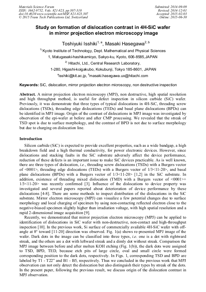
A mirror projection electron microscopy (MPJ), non destructive, high spatial resolution and high throughput method, is useful for defect inspection in silicon carbide (SiC) wafer. Previously, it was demonstrate that three type of typical dislocations in 4H-SiC, threading screw dislocation (TSD), threading edge dislocation (TED) and basal plane dislocations (BPD) can be identified in MPJ image. Origin of the contrast of dislocations in MPJ image was revealed by observation of the same wafer at as-grown and after CMP processing. Streak of TSD spot is due to surface morphology, and the contrast of BPD isn’t due to surface morphology but due to charging on dislocation line.

You might also be interested in these eBooks

Info:

Periodical:

Materials Science Forum (Volumes 821-823)

Pages:

307-310

Citation:

Online since:

June 2015

Export:

Price:

Permissions CCC:

Permissions PLS:

Сopyright:

© 2015 Trans Tech Publications Ltd. All Rights Reserved

Share:

Citation:

* - Corresponding Author

[1] P. G. Neudeck, Mater. Sci. Forum 338-342 (2000) 1161-1164.

Google Scholar

[2] T. Ohno, H. Yamaguchi, S. Kuroda, K. Kojima, T. Suzuki, K. Arai, J. Cryst. Growth 260 (2004) 209-216.

Google Scholar

[3] Y. Yao, Y. Ishikawa, Y. Sugawara, K. Sato, K. Danno, H. Suzuki, H. Sakamoto, T. Bessho, S. Yamaguchi, K. Nishikawa, Materials Science Forum; 2014, 778-780, (2014) 346-369.

DOI: 10.4028/www.scientific.net/msf.778-780.346

Google Scholar

[4] J. Senzaki, K. Kojima, T. Kato, A. Shimozato, K. Fukuda, Appl. Phys. Lett. 89 (2006) 022909.

DOI: 10.1063/1.2221525

Google Scholar

[5] U. Zimmermann, J. Österman, D. Kuylenstierns, A. Hallén, A. O. Konstantinov, V. M. Vetter M. Dudley: J. Appl. Phys. 93 (2003) 611-618.

Google Scholar

[6] T. Tsuji, T. Tawara, R. Tanuma, Y. Yonezawa, N. Iwamuro, K. Kosaka, H. Yurimoto, S. Kobayashi, H. Matsuhata, K. Fukuda, H. Okumura K. Arai, Mater. Sci. Forum 645-648 (2010) 913-916.

DOI: 10.4028/www.scientific.net/msf.645-648.913

Google Scholar

[7] J.P. Bergman, H. Lendenmann, P.A. Nilsson, P. Skytt: Mater. Sci. Forum 353-356 (2001), p.229.

Google Scholar

[8] J. J. Sumakeris, J. P. Bergman, M. K. Das, C. Hallin, B. A. Hull, E. Janzen, H. Lendenmann, M. J. O'Loughlin, M. J. Paisley, S. Ha, M. Skowroski, J. W. Palmour, C. H. Eddy Jr., Appl. Phys. Lett. 94 (2009) 041916.

Google Scholar

[9] M. Hasegawa, Abs. Int. Conf. Frontiers of Characterization and Metrology for Nanoelectronics 2013, Maryland, USA (2013) pp.158-160.

Google Scholar

[10] T. Isshiki, M. Hasegawa, Mater. Sci. Forum 778-780 (2014) 402-406.

Google Scholar

[11] Y. Orai, S. Watanabe, T. Sato, T. Isshiki, M. Fukui, Material Science Forum (in this issue).

Google Scholar