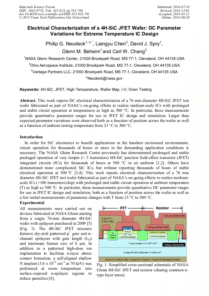
Electrical Characterization of a 4H-SiC JFET Wafer: DC Parameter Variations for Extreme Temperature IC Design

Article Preview

Abstract:

This work reports DC electrical characterization of a 76 mm diameter 4H-SiC JFET test wafer fabricated as part of NASA’s on-going efforts to realize medium-scale ICs with prolonged and stable circuit operation at temperatures as high as 500 °C. In particular, these measurements provide quantitative parameter ranges for use in JFET IC design and simulation. Larger than expected parameter variations were observed both as a function of position across the wafer as well as a function of ambient testing temperature from 23 °C to 500 °C.

You might also be interested in these eBooks

Info:

Periodical:

Materials Science Forum (Volumes 821-823)

Pages:

781-784

Citation:

Online since:

June 2015

Export:

Price:

Permissions CCC:

Permissions PLS:

Сopyright:

© 2015 Trans Tech Publications Ltd. All Rights Reserved

Share:

Citation:

* - Corresponding Author

[1] D. J. Spry et al., Materials Science Forum 600-603, 1079 (2008).

Google Scholar

[2] P. G. Neudeck et al., Physica Status Solidi A 206, 2329 (2009).

Google Scholar

[3] C. -P. Chen et al., 2014 IMAPS Int. Conf. on High Temperature Electronics, p.72 (2014).

Google Scholar

[4] L. Lanni, B. G. Malm, M. Ostling and C. -M. Zetterling, this conference.

Google Scholar

[5] Cree, Inc., http: /www. cree. com.

Google Scholar

[6] P. G. Neudeck, U. S. Patent No. 7, 935, 601 (3 May 2011).

Google Scholar

[7] M. J. Krasowski, U. S. Patent No. 7. 688, 117 (30 March 2010).

Google Scholar

[8] L. -Y. Chen and J. -F. Lei, Packaging of Harsh Environment MEMS Devices, in: M. Gad-el. Hak (Ed. ), MEMS Design and Fabrication, CRC Press, Boca Raton, Florida USA, 2006, pp.12-1.

Google Scholar

[9] R. S. Okojie, D. Lukco, Y. L. Chen, and D. J. Spry, J. Appl. Phys. 91, 6553 (2002).

Google Scholar

[10] C. J. Scozzie, F. B. McLean, and J. M. McGarrity, J. Appl. Phys. 81, 7687 (1997).

Google Scholar