Low Density of Near-Interface Traps at the Al2O3/4H-SiC Interface with Al2O3 Made by Low Temperature Oxidation of Al

Article Preview

Abstract:

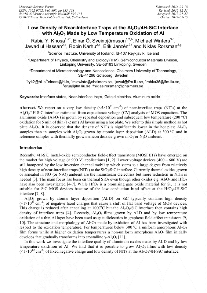
We report on a very low density (<5×1011 cm-2) of near-interface traps (NITs) at the Al2O3/4H-SiC interface estimated from capacitance-voltage (CV) analysis of MOS capacitors at different temperatures. The aluminum oxide (Al2O3) is grown by repeated deposition and subsequent low temperature (200°C) oxidation for 5 min of thin (1-2 nm) Al layers using a hot plate. We refer to this simple method as hot plate Al2O3. It is observed that the density of NITs is significantly lower in the hot plate Al2O3 samples than in samples with Al2O3 grown by atomic layer deposition (ALD) at 300°C and in reference samples with thermally grown silicon dioxide grown in O2 or N2O ambient.

You might also be interested in these eBooks

Info:

Periodical:

Pages:

135-138

Citation:

Online since:

May 2017

Export:

Price:

Permissions CCC:

Permissions PLS:

Сopyright:

© 2017 Trans Tech Publications Ltd. All Rights Reserved

Share:

Citation:

* - Corresponding Author

[1] www. wolfspeed. com.

Google Scholar

[2] www. rohm. com.

Google Scholar

[3] T. Kimoto, Japanese Journal of Applied Physics 54 (2015) 040103 and references therein.

Google Scholar

[4] M. Avice, U. Grossner, I. Pintilie, B. G. Svensson, M. Servidori, R. Nipoti, O. Nilsen and H. Fjellvag, Journal of Applied Physics 102 (2007) 054513.

DOI: 10.1063/1.2778289

Google Scholar

[5] T. Hatayama, S. Hino, N. Miura, T. Oomori and E. Tokumitsu, IEEE Transactions on Electron Devices 55 (2008) (2041).

Google Scholar

[6] C. M. Tanner, Y. C. Perng, C. Frewin, S. E. Saddow and J. P. Chang, Applied Physics Letters 91 (2007) 203510.

Google Scholar

[7] A. Taube, S. Gierałtowska, T. Gutt, T. Małachowski, I. Pasternak, T. Wojciechowski, W. Rzodkiewicz, M. Sawicki, A. Piotrowska, Acta Physica Polonica A 119 (2011) 696-698.

DOI: 10.12693/aphyspola.119.696

Google Scholar

[8] H. W. Chen, F. C. Chiu, C. H. Liu, S. Y. Chen, H. S. Huang, P. C. Juan and H. L. Hwang, Applied Surface Science 254 (2008) 6112–6115.

DOI: 10.1016/j.apsusc.2008.02.191

Google Scholar

[9] Z. Feng, C. Yu, J. Li, Q. Liu, Z. He, X. Song, J. Wang and S. Cai, Carbon 75 (2014) 249.

Google Scholar

[10] A. Badmaev, Y. Che, Z. Li, C. Wang and C. Zhou, ACS Nano 6 (2012) 3371.

Google Scholar

[11] L. P. H. Jeurgens, W. G. Sloof, F. D. Tichelaar and E. J. Mittemeijer, Thin Solid Films 418 (2002) 89.

DOI: 10.1016/s0040-6090(02)00787-3

Google Scholar

[12] T.E. Rudenko, I.N. Osiyuk, I.P. Tyagulski, H.Ö. Ólafsson and E.Ö. Sveinbjӧrnsson, Solid State Electronics 49 (2005) 545-553.

DOI: 10.1016/j.sse.2004.12.006

Google Scholar

[13] F. Allerstam, G. Gudjonsson, H.Ö. Ólafsson, E.Ö. Sveinbjörnsson, T. Rödle and R. Jos, Semiconductor Science and Technology 22 (2007) 307.

DOI: 10.1088/0268-1242/22/4/002

Google Scholar