p.143
p.151
p.155
p.159
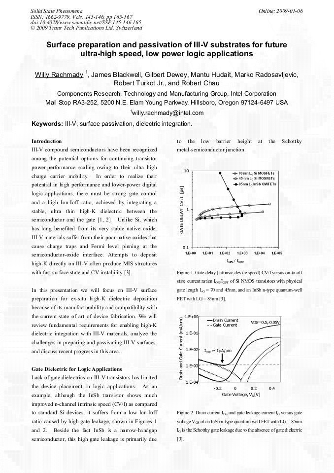
p.165
p.169
p.173
p.177
p.181
Surface Preparation and Passivation of III-V Substrates for Future Ultra-High Speed, Low Power Logic Applications

Abstract:
III-V compound semiconductors have been recognized among the potential options for continuing transistor power-performance scaling owing to their ultra high charge carrier mobility. In order to realize their potential in high performance and lower-power digital logic applications, there must be strong gate control and a high Ion-Ioff ratio, achieved by integrating a stable, ultra thin high-K dielectric between the semiconductor and the gate [1, 2]. Unlike Si, which has long benefited from its very stable native oxide, III-V materials suffer from their poor native oxides that cause charge traps and Fermi level pinning at the semiconductor-oxide interface. Attempts to deposit high-K directly on III-V often produce MIS structures with fast surface state and CV instability [3].
Info:
Periodical:
Pages:
165-167
Citation:
Online since:
January 2009
Keywords:
Price:
Сopyright:
© 2009 Trans Tech Publications Ltd. All Rights Reserved
Share:
Citation: