p.169
p.173
p.177
p.181
p.185
p.189
p.193
p.197
p.203
Defects of Silicon Substrates Caused by Electro-Static Discharge in Single Wafer Cleaning Process

Abstract:
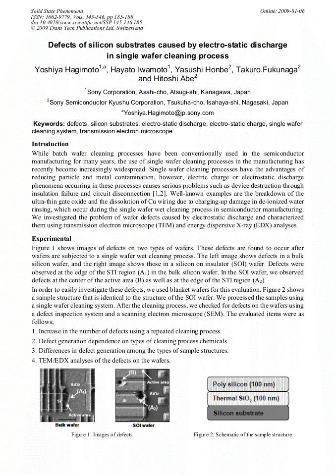
While batch wafer cleaning processes have been conventionally used in the semiconductor manufacturing for many years, the use of single wafer cleaning processes in the manufacturing has recently become increasingly widespread. Single wafer cleaning processes have the advantages of reducing particle and metal contamination, however, electric charge or electrostatic discharge phenomena occurring in these processes causes serious problems such as device destruction through insulation failure and circuit disconnection [1,2]. Well-known examples are the breakdown of the ultra-thin gate oxide and the dissolution of Cu wiring due to charging-up damage in de-ionized water rinsing, which occur during the single wafer wet cleaning process in semiconductor manufacturing. We investigated the problem of wafer defects caused by electrostatic discharge and characterized them using transmission electron microscope (TEM) and energy dispersive X-ray (EDX) analyses.
Info:
Periodical:
Pages:
185-188
Citation:
Online since:
January 2009
Price:
Сopyright:
© 2009 Trans Tech Publications Ltd. All Rights Reserved
Share:
Citation: