p.213
p.217
p.221
p.225
p.233
p.237
p.241
p.247
p.251
The Role of Mass Transfer in Removal of Cross-Linked Sacrificial Layers in 3DI Applications

Abstract:
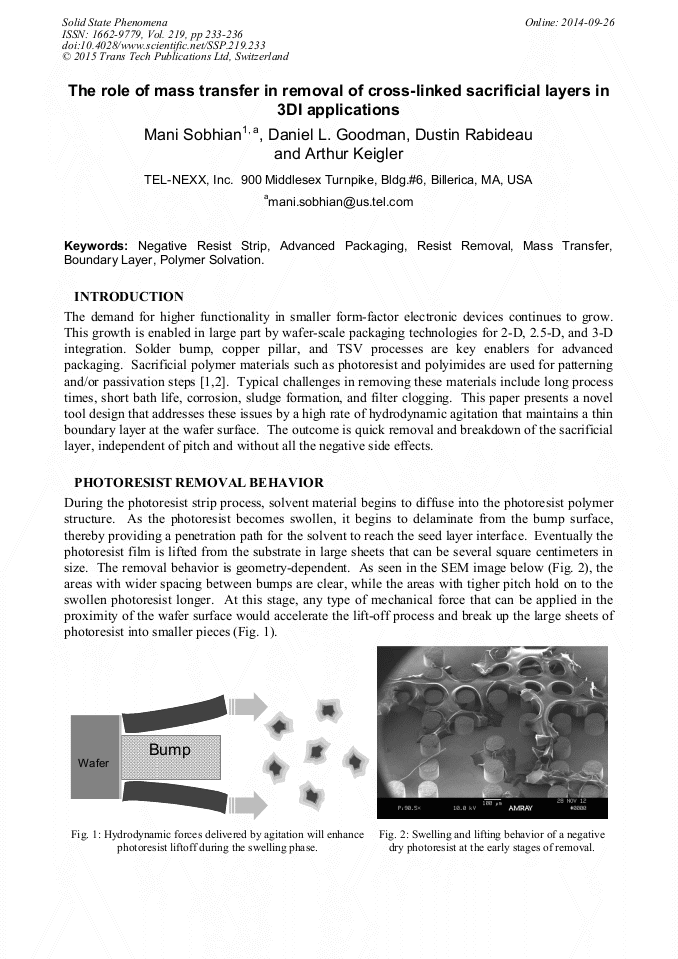
The demand for higher functionality in smaller form-factor electronic devices continues to grow. This growth is enabled in large part by wafer-scale packaging technologies for 2-D, 2.5-D, and 3-D integration. Solder bump, copper pillar, and TSV processes are key enablers for advanced packaging. Sacrificial polymer materials such as photoresist and polyimides are used for patterning and/or passivation steps [1,2]. Typical challenges in removing these materials include long process times, short bath life, corrosion, sludge formation, and filter clogging. This paper presents a novel tool design that addresses these issues by a high rate of hydrodynamic agitation that maintains a thin boundary layer at the wafer surface. The outcome is quick removal and breakdown of the sacrificial layer, independent of pitch and without all the negative side effects.
Info:
Periodical:
Pages:
233-236
DOI:
Citation:
Online since:
September 2014
Authors:
Price:
Сopyright:
© 2015 Trans Tech Publications Ltd. All Rights Reserved
Share:
Citation: