InGaAs (110) Surface Cleaning Using Atomic Hydrogen

Article Preview

Abstract:

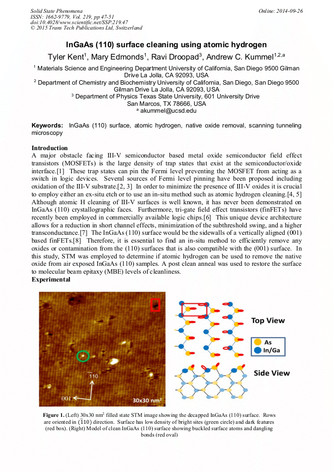
A major obstacle facing III-V semiconductor based metal oxide semiconductor field effect transistors (MOSFETs) is the large density of trap states that exist at the semiconductor/oxide interface.[1] These trap states can pin the Fermi level preventing the MOSFET from acting as a switch in logic devices. Several sources of Fermi level pinning have been proposed including oxidation of the III-V substrate.[2, 3] In order to minimize the presence of III-V oxides it is crucial to employ either an ex-situ etch or to use an in-situ method such as atomic hydrogen cleaning.[4, 5] Although atomic H cleaning of III-V surfaces is well known, it has never been demonstrated on InGaAs (110) crystallographic faces. Furthermore, tri-gate field effect transistors (finFETs) have recently been employed in commercially available logic chips.[6] This unique device architecture allows for a reduction in short channel effects, minimization of the subthreshold swing, and a higher transconductance.[7] The InGaAs (110) surface would be the sidewalls of a vertically aligned (001) based finFETs.[8] Therefore, it is essential to find an in-situ method to efficiently remove any oxides or contamination from the (110) surfaces that is also compatible with the (001) surface. In this study, STM was employed to determine if atomic hydrogen can be used to remove the native oxide from air exposed InGaAs (110) samples. A post clean anneal was used to restore the surface to molecular beam epitaxy (MBE) levels of cleanliness.

You might also be interested in these eBooks

Info:

Periodical:

Solid State Phenomena (Volume 219)

Pages:

47-51

Citation:

Online since:

September 2014

Export:

Price:

Permissions CCC:

Permissions PLS:

Сopyright:

© 2015 Trans Tech Publications Ltd. All Rights Reserved

Share:

Citation:

* - Corresponding Author

[1] Mönch, W., Semiconductor surfaces and interfaces. Vol. 26. 2001: Springer. Robertson, J., Model of interface states at III-V oxide interfaces. Applied Physics Letters, 2009. 94(15): p.152104.

DOI: 10.1063/1.3120554

Google Scholar

[2] Hasegawa, H., et al., Surface passivation of III–V semiconductors for future CMOS devices—Past research, present status and key issues for future. Applied surface science, 2010. 256(19): pp.5698-5707.

DOI: 10.1016/j.apsusc.2010.03.091

Google Scholar

[3] Williams, K.R. and R.S. Muller, Etch rates for micromachining processing. Microelectromechanical Systems, Journal of, 1996. 5(4): pp.256-269.

DOI: 10.1109/84.546406

Google Scholar

[4] Melitz, W., et al., InGaAs surface preparation for atomic layer deposition by hydrogen cleaning and improvement with high temperature anneal. Journal of Applied Physics, 2011. 110(1): p.013713.

DOI: 10.1063/1.3597791

Google Scholar

[5] Auth, C., et al. A 22nm high performance and low-power CMOS technology featuring fully-depleted tri-gate transistors, self-aligned contacts and high density MIM capacitors. in VLSI Technology (VLSIT), 2012 Symposium on. 2012. IEEE.

DOI: 10.1109/vlsit.2012.6242496

Google Scholar

[6] Hisamoto, D., et al. A fully depleted lean-channel transistor (DELTA)-a novel vertical ultra thin SOI MOSFET. in Electron Devices Meeting, 1989. IEDM'89. Technical Digest., International. 1989. IEEE.

DOI: 10.1109/iedm.1989.74182

Google Scholar

[7] Jurczak, M., et al. Review of FINFET technology. in SOI Conference, 2009 IEEE International. 2009. IEEE.

Google Scholar

[8] Tomkiewicz, P., A. Winkler, and J. Szuber, Comparative study of the GaAs (100) surface cleaned by atomic hydrogen. Applied surface science, 2006. 252(21): pp.7647-7658.

DOI: 10.1016/j.apsusc.2006.03.060

Google Scholar

[9] Horikoshi, Y., M. Kawashima, and H. Yamaguchi, Photoluminescence characteristics of AlGaAs‐GaAs single quantum wells grown by migration‐enhanced epitaxy at 300 °C substrate temperature. Applied Physics Letters, 1987. 50(23): pp.1686-1687.

DOI: 10.1063/1.97768

Google Scholar

[10] Horikoshi, Y., et al., Growth process of III–V compound semiconductors by migration-enhanced epitaxy. Journal of crystal growth, 1990. 105(1): pp.326-338.

DOI: 10.1016/0022-0248(90)90382-u

Google Scholar

[11] Aguirre-Tostado, F., et al., Indium stability on InGaAs during atomic H surface cleaning. Applied Physics Letters, 2008. 92(17): pp.171906-3.

DOI: 10.1063/1.2919047

Google Scholar