p.47
p.52
p.56
p.59
p.63
p.68
p.73
p.78
p.81
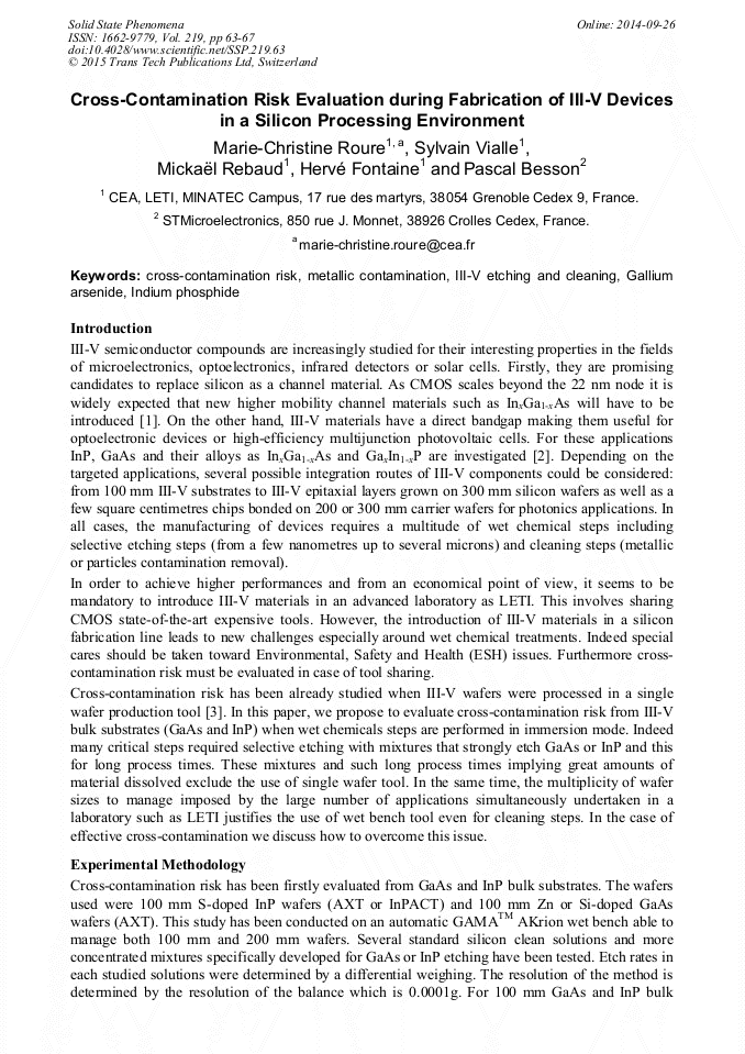
Cross-Contamination Risk Evaluation during Fabrication of III-V Devices in a Silicon Processing Environment
Abstract:
III-V semiconductor compounds are increasingly studied for their interesting properties in the fields of microelectronics, optoelectronics, infrared detectors or solar cells. Firstly, they are promising candidates to replace silicon as a channel material. As CMOS scales beyond the 22 nm node it is widely expected that new higher mobility channel materials such as InxGa1-xAs will have to be introduced [1]. On the other hand, III-V materials have a direct bandgap making them useful for optoelectronic devices or high-efficiency multijunction photovoltaic cells. For these applications InP, GaAs and their alloys as InxGa1-xAs and GaxIn1-xP are investigated [2]. Depending on the targeted applications, several possible integration routes of III-V components could be considered: from 100 mm III-V substrates to III-V epitaxial layers grown on 300 mm silicon wafers as well as a few square centimetres chips bonded on 200 or 300 mm carrier wafers for photonics applications. In all cases, the manufacturing of devices requires a multitude of wet chemical steps including selective etching steps (from a few nanometres up to several microns) and cleaning steps (metallic or particles contamination removal).
Info:
Periodical:
Pages:
63-67
DOI:
Citation:
Online since:
September 2014
Price:
Сopyright:
© 2015 Trans Tech Publications Ltd. All Rights Reserved
Share:
Citation:


