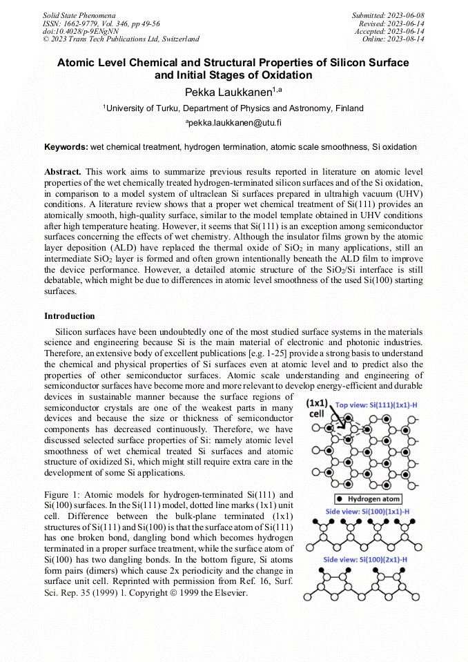
[1]
Y. J. Chabal, K. Raghavachari, New ordered structure for the H-saturated Si(100) surface: The (3×1) phase, Phys. Rev. Lett. 54 (1985) 1055.
DOI: 10.1103/physrevlett.54.1055
Google Scholar
[2]
K. Takayanagi, Y. Tanishiro, S. Takahashi, M. Takahashi, Structure analysis of Si(111)-7×7 reconstructed surface by transmission electron diffraction, Surf. Sci. 164 (1985) 367.
DOI: 10.1016/0039-6028(85)90753-8
Google Scholar
[3]
R. I. G. Uhrberg, G. V. Hansson, U. O. Karlsson, J. M. Nicholls, P. E. S. Persson, S. A. Flodström, R. Engelhardt, E.-E. Koch, Bulk and surface electronic structures of Si(111)2×1 and Si(111)7×7 studied by angle-resolved photoelectron spectroscopy, Phys. Rev. B 31 (1985) 3795.
DOI: 10.1103/physrevb.31.3795
Google Scholar
[4]
E. Yablonovitch, D. L. Allara, C. C. Chang, T. Gmitter, T. B. Bright, Unusually low surface-recombination velocity on silicon and germanium surfaces, Phys. Rev. Lett. 57 (1986) 249.
DOI: 10.1103/physrevlett.57.249
Google Scholar
[5]
A. Ishizaka, Y. Shiraki, Low temperature surface cleaning of silicon and its application to silicon MBE, J. Electrochem. Soc. 133 (1986) 666.
DOI: 10.1149/1.2108651
Google Scholar
[6]
R. J. Hamers, R. M. Tromp, J. E. Demuth, Scanning tunneling microscopy of Si(001), Phys. Rev. B 34 (1986) 5343.
DOI: 10.1103/physrevb.34.5343
Google Scholar
[7]
T. Takahagi, I. Nagai, A. Ishitani, H. Kuroda, Nagasawa, The formation of hydrogen passivated silicon single-crystal surfaces using ultraviolet cleaning and HF etching, J. Appl. Phys. 64 (1988) 3516.
DOI: 10.1063/1.341489
Google Scholar
[8]
W. Kern, The evolution of silicon wafer cleaning technology, J. Electrochem. Soc. 137 (1990) 1887.
Google Scholar
[9]
R. A. Wolkow, Direct observation of an increase in buckled dimers on Si(001) at low temperature, Phys. Rev. Lett. 68 (1992) 2636.
DOI: 10.1103/physrevlett.68.2636
Google Scholar
[10]
T. Engel, The interaction of molecular and atomic oxygen with Si(100) and Si(111), Surf. Sci. Rep. 18 (1993) 93.
Google Scholar
[11]
E. Pehlke, M. Scheffler, Evidence for site-sensitive screening of core holes at the Si and Ge (001) surface, Phys. Rev. Lett. 71 (1993) 2338.
DOI: 10.1103/physrevlett.71.2338
Google Scholar
[12]
M. Meuris, P. W. Mertens, A. Opdebeeck, H. F. Schmidt, M. Depas, G. Vereecke, The IMEC clean: a new concept for particle and metal removal on Si surfaces, Sol. State Technol. 38 (1995) 109.
Google Scholar
[13]
Y. Morita, H. Tokumoto, Ideal hydrogen termination of Si(001) surface by wetchemical preparation, Appl. Phys. Lett. 67 (1995) 2654.
DOI: 10.1063/1.114326
Google Scholar
[14]
Proceedings of the fourth international symposium on cleaning technology in semiconductor device manufacturing. Edited by R. E. Novak, J. Ruzyllo, C. M. Appel, T. Hattori, M. M. Heyns, Electrochemical Society Proceedings 95-20 (1996).
Google Scholar
[15]
K. Endo, K. Arima, T. Kataoka, Y. Oshikane, H. Inoue, Y. Mori, Atomic structures of hydrogen-terminated Si(001) surfaces after wet cleaning by scanning tunneling microscopy, Appl. Phys. Lett. 73 (1998) 1853.
DOI: 10.1063/1.122304
Google Scholar
[16]
K. Oura, V. G. Lifshits, A. A. Saranin, A. V. Zotov, M. Katayama, Hydrogen interaction with clean and modied silicon surfaces, Surf. Sci. Rep. 35 (1999) 1.
DOI: 10.1016/s0167-5729(99)00005-9
Google Scholar
[17]
T. Takahagi, S. Shingubara, H. Sakaue, Wet preparation of defect-free hydrogen-terminated silicon wafer surface and its characterization in atomic-scale. 5th International Symposium on Ultra Clean Processing of Silicon Surfaces (UCPSS 2000), Sol. State Phenom. 76-77 (2001) 105.
DOI: 10.4028/www.scientific.net/ssp.76-77.105
Google Scholar
[18]
H. Sakaue, S. Fujiwara, S. Shingubara, T. Takahagi, Atomic-scale defect control on hydrogen-terminated silicon surface at wafer scale, Appl. Phys. Lett. 78 (2001) 309.
DOI: 10.1063/1.1339993
Google Scholar
[19]
F. De Smedt, S. De Gendt, M. Claes, M.M. Heyns, H. Vankerckhoven, C. Vinckier, The increasing importance of the use of ozone in the microelectronics industry, Ozone Sci. Engineer. 24 (2002) 379.
DOI: 10.1080/01919510208901628
Google Scholar
[20]
H. Sakaue, Y. Taniguchi, Y. Okamura, S. Shingubara T. Takahagi, Wet treatment for preparing atomically smooth Si(100) wafer surface, Appl. Surf. Sci. 234 (2004) 439.
DOI: 10.1016/j.apsusc.2004.05.052
Google Scholar
[21]
B. Onsia, M. Caymax, T. Conard, S. De Gendt, F. De Smedt, A. Delabie, C. Gottschalk, M. Green, M. Heyns, S. Lin, P. Mertens, W. Tsai, C. Vinckier, On the application of a thin ozone based wet chemical oxide as an interface for ALD high-k deposition, Diff. Defect Data Pt.B: Sol. State Phenom. (2005).
DOI: 10.4028/www.scientific.net/ssp.103-104.19
Google Scholar
[22]
G.-H. Lu, M. Huang, M. Cuma, F. Liu, Relative stability of Si surfaces: A first-principles study, Surf. Sci. 588 (2005) 61.
DOI: 10.1016/j.susc.2005.05.028
Google Scholar
[23]
K. Arima, J. Katoh, S. Horie, K. Endo, T. Ono, S. Sugawa, H. Akahori, A. Teramoto, T. Ohmi, Hydrogen termination of Si(110) surfaces upon wet cleaning revealed by highly resolved scanning tunneling microscopy, J. Appl. Phys. 98 (2005) 103525.
DOI: 10.1063/1.2136214
Google Scholar
[24]
H. Kato, T. Taoka, S. Nishikata, G. Sazaki, T. Yamada, R. Czajka, A Wawro, K. Nakajima, A. Kasuya, S. Suto, Preparation of an ultraclean and atomically controlled hydrogen-terminated Si(111)-(1x1) surface revealed by high resolution electron energy loss spectroscopy, atomic force microscopy, and scanning tunneling microscopy: Aqueous NH4F etching process of Si(111), Jpn. J. Appl. Phys. 46 (2007) 5701.
DOI: 10.1143/jjap.46.5701
Google Scholar
[25]
T. Yamasaki, K. Kato, T. Uda, T. Yamamoto, T. Ohno, First-principles theory of Si(110)-(16×2) surface reconstruction for unveiling origin of pentagonal scanning tunneling microscopy images, Appl. Phys. Express 9 (2016) 035501.
DOI: 10.7567/apex.9.035501
Google Scholar
[26]
A. Ourmazd, D. W. Taylor, J. A. Rentschler, J. Bevk, Si®SiO2 transformation: Interfacial structure and mechanism, Phys. Rev. Lett. 59 (1987) 213.
DOI: 10.1103/physrevlett.59.213
Google Scholar
[27]
A. Munkholm, S. Brennan, F. Comin, L. Ortega, Observation of a distributed epitaxial oxide in thermally grown SiO2 on Si(001), Phys. Rev. Lett. 75 (1995) 4254.
DOI: 10.1103/physrevlett.75.4254
Google Scholar
[28]
Y. Wei, R. M. Wallace, A. C. Seabaugh, Void formation on ultrathin thermal silicon oxide films on the Si(100) surface, Appl. Phys. Lett. 69 (1996) 1270.
DOI: 10.1063/1.117388
Google Scholar
[29]
Z. H. Lu, J. P. McCaffrey, B. Brar, G. D. Wilk, R. M. Wallace, L. C. Feldman, S. P. Tay, SiO2 film thickness metrology by x-ray photoelectron spectroscopy, Appl. Phys. Lett. 71 (1997) 2764.
DOI: 10.1063/1.120438
Google Scholar
[30]
H. Kageshima, K. Shiraishi, First-principles study of oxide growth on Si(100) surfaces and at SiO2/Si(100) interfaces, Phys. Rev. Lett. 81 (1998) 5936.
DOI: 10.1103/physrevlett.81.5936
Google Scholar
[31]
A. Stesmans, V. V. Afanas'ev, Electron spin resonance features of interface defects in thermal (100)Si/SiO2, J. Appl. Phys. 83 (1998) 2449.
DOI: 10.1063/1.367005
Google Scholar
[32]
Y. Tu, J. Tersoff, Structure and energetics of the Si-SiO2 interface, Phys. Rev. Lett. 84 (2000) 4393.
Google Scholar
[33]
J. H. Oh, H. W. Yeom, Y. Hagimoto, K. Ono, and M. Oshima, N. Hirashita, M. Nywa, A. Toriumi, A. Kakizaki, Chemical structure of the ultrathin SiO2/Si(100) interface: An angle-resolved Si 2p photoemission study, Phys. Rev. B 63 (2001) 205310.
DOI: 10.1103/physrevb.63.205310
Google Scholar
[34]
Fundamental Aspects of Silicon Oxidation edited by Y. J. Chabal (2001) Springer.
Google Scholar
[35]
A. Bongiorno, A. Pasquarello, M. S. Hybertsen, L. C. Feldman, Transition structure at the Si(100)-SiO2 interface, Phys. Rev. Lett. 90 (2003) 186101.
Google Scholar
[36]
T. Yamasaki, K. Kato, T. Uda, Oxidation of the Si(001) surface: lateral growth and formation of Pb0 centers, Phys. Rev. Lett. 91 (2003) 146102.
Google Scholar
[37]
S. Imai, S. Mizushima, W. B. Kim, H. Kobayashi, Properties of thick SiO2/Si structure formed at 120 C by use of two-step nitric acid oxidation method, Appl. Surf. Sci. 254 (2008) 8054.
DOI: 10.1016/j.apsusc.2008.03.025
Google Scholar
[38]
G. Dingemans, M. C. M. van de Sanden, W. M. M. Kessels, Excellent Si surface passivation by low temperature SiO2 using an ultrathin Al2O3 capping film, Phys. Status Sol. RRL 5 (2011) 22.
DOI: 10.1002/pssr.201004378
Google Scholar
[39]
A. Laades, H. Angermann, H.-P. Sperlich, U. Stürzebecher, C. A. D. Álvarez, M. Bähr, A. Lawerenz 2013 Wet chemical oxidation of silicon surfaces prior to the deposition of all PECVD AlOx/a-SiNx passivation stacks for silicon solar cells, Sol. State Phenom. 195 (2013) 310.
DOI: 10.4028/www.scientific.net/ssp.195.310
Google Scholar
[40]
M. A. Juntunen, J. Heinonen, V. Vähänissi, P. Repo, D. Valluru, H. Savin, Near-unity quantum efficiency of broadband black silicon photodiodes with an induced junction, Nat. Photon. 10 (2016) 777.
DOI: 10.1038/nphoton.2016.226
Google Scholar
[41]
M. Köhler, M. Pomaska, F. Lentz, F. Finger, U. Rau, K. Ding, Wet-chemical preparation of silicon tunnel oxides for transparent passivated contacts in crystalline silicon solar cells, ACS Appl. Mat. & Int. 10 (2018) 14259.
DOI: 10.1021/acsami.8b02002
Google Scholar
[42]
S. S. Cheema, N. Shanker, L. C. Wang, C. H. Hsu, S. L. Hsu, Y. H. Liao, M. S. Jose, J. Gomez, W. Chakraborty, W. Li, J. H. Bae, S. K. Volkman, D. Kwon, Y. Rho, G. Pinelli, R. Rastogi, D. Pipitone, C. Stull, M. Cook, B. Tyrrell, V. A. Stoica, Z. Zhang, J. W. Freeland, C. J. Tassone, A. Mehta, G. Saheli, D. Thompson, D. I. Suh, W. T. Koo, K. J. Nam, D. J. Jung, W. B. Song, C. H. Lin, S. Nam, J. Heo, N. Parihar, C. P. Grigoropoulos, P. Shafer, P. Fay, R. Ramesh, S. Mahapatra, J. Ciston, S. Datta, M. Mohamed, C. Hu, S. Salahuddin, Ultrathin ferroic HfO2-ZrO2 superlattice gate stack for advanced transistors, Nature 604 (2022) 6.
DOI: 10.1038/s41586-022-04425-6
Google Scholar
[43]
S. Bakhshi, N. Zin, H. Ali, M. Wilson, D. Chanda, K. O. Davis, W. V. Schoenfeld, Simple and versatile UV-ozone oxide for silicon solar cell applications, Sol. Energy Mat. Sol. Cells 185 (2018) 505.
DOI: 10.1016/j.solmat.2018.06.006
Google Scholar
[44]
E. P. Gusev, H. C. Lu, T. Gustafsson, E. Garfunkel, Growth mechanism of thin silicon oxide films on Si(100) studied by medium-energy ion scattering, Phys. Rev. B 52 (1995) 1759.
DOI: 10.1103/physrevb.52.1759
Google Scholar
[45]
H. Angermann, T. Dittrich, H. Flietner, Investigation of native-oxide growth on HF-treated Si(111) surfaces by measuring the surface-state distribution, Appl. Phys. A Sol. Surf. 59 (1994) 193.
DOI: 10.1007/bf00332216
Google Scholar
[46]
B. J. Hallam, P. G. Hamer, A. M. C. née Wenham, C. E. Chan, B. V. Stefani, S. Wenham, Development of advanced hydrogenation processes for silicon solar cells via an improved understanding of the behaviour of hydrogen in silicon, Progr. Photov. 28 (2020) 1217.
DOI: 10.1002/pip.3240
Google Scholar
[47]
M. U. Khan, D. Chen, S. Jafari, T. Ohshima, H. Abe, Z. Hameiri, C. M. Chong, M. Abbott Degradation and regeneration of radiation-induced defects in silicon: A study of vacancy-hydrogen, Sol. Energy Mat. Sol. Cells 200 (2019) 109990.
DOI: 10.1016/j.solmat.2019.109990
Google Scholar
[48]
A.-M. El-Sayed, Y. Wimmer, W. Goes, T. Grasser, V. V. Afanas'ev, A. L. Shluger, Theoretical models of hydrogen-induced defects in amorphous silicon dioxide, Phys. Rev. B 92 (2015) 014107.
DOI: 10.1103/physrevb.92.014107
Google Scholar
[49]
M. Kuzmin, J.-P. Lehtiö, J. Mäkelä, M. Yasir, Z. J. Rad, E. Vuorinen, A. Lahti, M. Punkkinen, P. Laukkanen, K. Kokko, H.-P. Hedman, R. Punkkinen, M. Lastusaari, P. Repo, H. Savin, Observation of crystalline oxidized silicon phase, Adv. Mater. Interf. 6 (2019) 1802033.
DOI: 10.1002/admi.201802033
Google Scholar
[50]
Z. J. Rad, J-P. Lehtiö, I. Mack, K. Rosta, K. Chen, V. Vähänissi, M. Punkkinen, R. Punkkinen, H-P. Hedman, A. Pavlov, M. Kuzmin, H. Savin, P. Laukkanen, K. Kokko, Decreasing interface defect densities via silicon oxide passivation at temperatures below 450C, ACS Appl. Mat. Interf. 12 (2020) 46933.
DOI: 10.1021/acsami.0c12636
Google Scholar
[51]
Z. J. Rad, J.-P. Lehtiö, K. Chen, I. Mack, V. Vähänissi, M. Punkkinen, R. Punkkinen, H.-P. Hedman, M. Kuzmin, H. Savin, P. Laukkanen, K. Kokko, Effects of post treatment of oxide-silicon interfaces in ultrahigh vacuum below 400 ºC, Vacuum 202 (2022) 111134.
DOI: 10.1016/j.vacuum.2022.111134
Google Scholar
[52]
G. D. Wilk, R. M. Wallace, B. P. S. Brar, Low temperature method for forming a thin, uniform oxide, Patent US7030038B1 (2006).
Google Scholar
[53]
G. D. Wilk, Y. Wei, H. Edwards, R. M. Wallace, In situ Si flux cleaning technique for producing atomically flat Si(100) surfaces at low temperature, Appl. Phys. Lett. 70 (1997) 2288.
DOI: 10.1063/1.119083
Google Scholar