Effect of Substrate Temperature on Properties of Silicon Nitride Films Deposited by RF Magnetron Sputtering

Article Preview

Abstract:

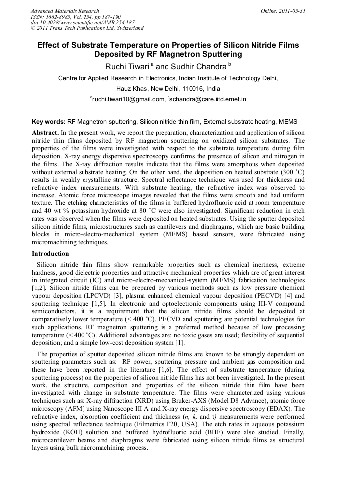
In the present work, we report the preparation, characterization and application of silicon nitride thin films deposited by RF magnetron sputtering on oxidized silicon substrates. The properties of the films were investigated with respect to the substrate temperature during film deposition. X-ray energy dispersive spectroscopy confirms the presence of silicon and nitrogen in the films. The X-ray diffraction results indicate that the films were amorphous when deposited without external substrate heating. On the other hand, the deposition on heated substrate (300 °C) results in weakly crystalline structure. Spectral reflectance technique was used for thickness and refractive index measurements. With substrate heating, the refractive index was observed to increase. Atomic force microscope images revealed that the films were smooth and had uniform texture. The etching characteristics of the films in buffered hydrofluoric acid at room temperature and 40 wt % potassium hydroxide at 80 °C were also investigated. Significant reduction in etch rates was observed when the films were deposited on heated substrates. Using the sputter deposited silicon nitride films, microstructures such as cantilevers and diaphragms, which are basic building blocks in micro-electro-mechanical system (MEMS) based sensors, were fabricated using micromachining techniques.

You might also be interested in these eBooks

Info:

Periodical:

Pages:

187-190

Citation:

Online since:

May 2011

Export:

Price:

Permissions CCC:

Permissions PLS:

Сopyright:

© 2011 Trans Tech Publications Ltd. All Rights Reserved

Share:

Citation:

[1] V. Bhatt and S. Chandra, Silicon nitride films deposited by RF sputtering for microstructure fabrication in MEMS, J. Electron. Mater. 28 (2009) 1979-1089.

DOI: 10.1007/s11664-009-0846-8

Google Scholar

[2] M. Vila, C. Prieto, P. Miranzo, M.I. Osendi and R. Ramirez, Characterization of silicon nitride thin films prepared by RF magnetron sputtering, Surf. Coat. Technol. 151-152 (2002) 67-71.

DOI: 10.1016/s0257-8972(01)01600-0

Google Scholar

[3] L.S. Zambom, R.D. Mansano, R. Furlan and P. Verdonck, LPCVD deposition of silicon nitride assisted by high density plasmas, Thin Solid Films. 343-344 (1999) 299-301.

DOI: 10.1016/s0040-6090(98)01587-9

Google Scholar

[4] M. Mikolajunas, R. Kaliasas, M. Andrulevicius, V. grigaliunas, J. Baltrusaitis and D. Virzonis, A study of stacked PECVD silicon nitride films used for surface micromachined membranes, Thin Solid Films. 516 (2008) 8788-8792.

DOI: 10.1016/j.tsf.2008.06.063

Google Scholar

[5] H. Liang, Q. Zhao, F. Gao, W. Yuan and Y. Dong, Effect of RF sputtering power on the structural, optical and hydrophobic properties of silicon nitride thin films, Advanced Materials Research. 194-196 (2011) 23-40.

DOI: 10.4028/www.scientific.net/amr.194-196.2340

Google Scholar

[6] S. A Awan and R.D. Gould, Conductivity and dielectric properties of silicon nitride thin films prepared by RF magnetron sputtering using nitrogen gas, Thin Solid Films. 423 (2003) 267-272.

DOI: 10.1016/s0040-6090(02)01049-0

Google Scholar

[7] K.R. Williams, K. Gupta and M. Wasilik, Etch rates for micromachining processing-part II, J. Microelectromechanical Systems. 12 (2003) 761-777.

DOI: 10.1109/jmems.2003.820936

Google Scholar