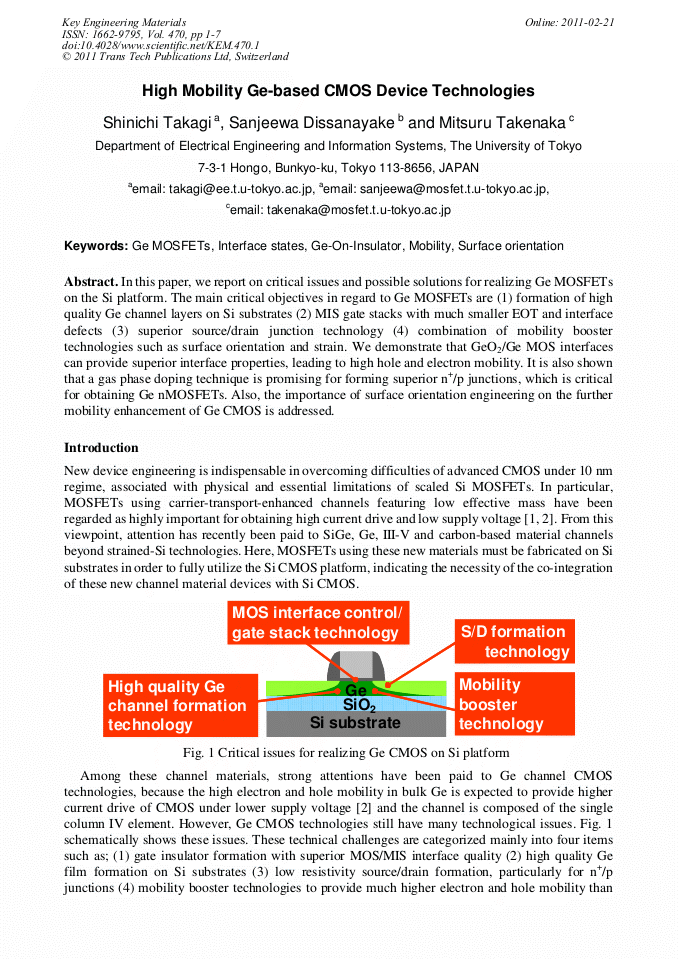
[1]
S. Takagi, T. Tezuka, T. Irisawa, S. Nakaharai, T. Numata, K. Usuda, N. Sugiyama, M. Shichijo, R. Nakane, S. Sugahara, Solid-State Electron., Vol. 51 (2007) p.526.
DOI: 10.1016/j.sse.2007.02.017
Google Scholar
[2]
S. Takagi, T. Irisawa, T. Tezuka, T. Numata, S. Nakaharai, N. Hirashita, Y. Moriyama, K. Usuda, E. Toyoda, S. Dissanayake, M. Shichijo, R. Nakane, S. Sugahara, M. Takenaka and N. Sugiyama, IEEE Trans. Electron Devices, Vol. 55 (2008) p.21.
DOI: 10.1109/ted.2007.911034
Google Scholar
[3]
D. Kuzum, A. J. Pethe, T. Krishnamohan, Y. Oshima, Y. Sun, J. P. McVittie, P. A. Pianetta, P. C. McIntyre, and K. C. Saraswat, International Electron Device Meeting Tech. Dig., (2007) p.723.
DOI: 10.1109/iedm.2007.4419048
Google Scholar
[4]
H. Shang, K. -L. Lee, P. Kozlowski, C. D'Emic, I. Babich, E. Sikorski, M. Ieong, H. -S. P. Wong, K. Guarini, and W. Haensch, IEEE Electron Device Lett., Vol. 25 (2004) p.135.
DOI: 10.1109/led.2003.823060
Google Scholar
[5]
S. J. Whang, S. J. Lee, F. Gao, N. Wu, C. X. Zhu, J. S. Pan, L. J. Tang, and D. L. Kwong, International Electron Device Meeting Tech. Dig., (2004) p.307.
Google Scholar
[6]
K. Martens, B. D. Jaeger, R. Bonzom, J. V. Steenbergen, M. Meuris, G. Groeseneken, and H. Maes, IEEE Electron Device Lett., Vol. 27 (2006) p.405.
DOI: 10.1109/led.2006.873767
Google Scholar
[7]
C. O. Chui, F. Ito, and K. C. Saraswat, IEEE Trans. Electron Devices, Vol. 53 (2006) p.1501.
Google Scholar
[8]
S. Takagi, T. Maeda, N. Taoka, M. Nishizawa, Y. Morita, K. Ikeda, Y. Yamashita, M. Nishikawa, H. Kumagai, R. Nakane, S. Sugahara and N. Sugiyama, Microelectron. Eng., Vol. 84, (2007) p.2314.
DOI: 10.1016/j.mee.2007.04.129
Google Scholar
[9]
H. Matsubara, T. Sasada, M. Takenaka and S. Takagi, Appl. Phys. Lett., Vol. 93 (2008) 032104.
Google Scholar
[10]
T. Sasada, Y. Nakakita, M. Takenaka and S. Takagi, J. Appl. Phys., Vol. 106 (2009) 073716.
Google Scholar
[11]
C. H. Lee, T. Tabata, T. Nishimura, K. Nagashio, K. Kita and A. Toriumi, Appl. Phys. Exp., Vol. 2 (2009) 071404.
Google Scholar
[12]
S. Takagi, N. Taoka and M. Takenaka, ECS Trans., Vol. 19 (2009) p.67.
Google Scholar
[13]
M. Houssa, G. Pourtois, M. Caymax, M. Meuris, M. M. Heyns, V. V. Afanas'ev and A. Stesmans, Appl. Phys. Lett., Vol. 93 (2008) 161909.
DOI: 10.1063/1.3006320
Google Scholar
[14]
K. Kita, S. Suzuki, H. Nomura, T. Takahashi, T. Nishimura and A. Toriumi, Jpn. J. Appl. Phys., Vol. 47 (2008) p.2349.
Google Scholar
[15]
Y. Nakakita, R. Nakane, T. Sasada, H. Matsubara, M. Takenaka and S. Takagi, International Electron Device Meeting Tech. Dig., (2008) p.877.
Google Scholar
[16]
K. Morii, T. Iwasaki, R. Nakane, M. Takenaka and S. Takagi, International Electron Device Meeting Tech. Dig. (2009) p.681.
Google Scholar
[17]
K. Morii, T. Iwasaki, R. Nakane, M. Takenaka, and S. Takagi, IEEE Electron Device Lett., Vol. 31 (2010) p.1092.
Google Scholar
[18]
M. Takenaka, M. Sugiyama, Y. Nakano and S. Takagi, European Material Research Society, Symposium I (2009) 14. 4.
Google Scholar
[19]
C. H. Lee, T. Nishimura, N. Saido, K. Nagashio, K. Kita and A. Toriumi, I International Electron Device Meeting Tech. Dig. (2009) p.457.
Google Scholar
[20]
T. Nishimura, C. H. Lee, S. K. Wang, T. Tabata, K. Kita, K. Nagashio and A. Toriumi, Proc. Symp. on VLSI Tech. (2010) p.209.
Google Scholar
[21]
T. Tezuka, N. Sugiyama, T. Mizuno, M. Suzuki, and S. Takagi, Jpn. J. Appl. Phys., Vol. 40 (2001) p.2866.
Google Scholar
[22]
S. Nakaharai, T. Tezuka, N. Sugiyama, Y. Moriyama and S. Takagi, Appl. Phys. Lett., Vol. 83 (2003) p.3516.
Google Scholar
[23]
S. Nakaharai, T. Tezuka, N. Hirashita, E. Toyoda, Y. Moriyama, N. Sugiyama and S. Takagi, J. Appl. Phys., Vol. 105 (2009) 024515.
DOI: 10.1063/1.3068339
Google Scholar
[24]
S. Nakaharai, T. Tezuka, E. Toyoda, N. Hirashita, Y. Moriyama, T. Maeda, T. Numata, N. Sugiyama, and S. Takagi, Ext. Abs. International Conference on Solid State Devices and Materials (2005) p.868.
DOI: 10.7567/ssdm.2005.b-7-3
Google Scholar
[25]
K. Ikeda, N. Taoka, Y. Yamashita, M. Harada, K. Suzuki, T. Yamamoto, N. Sugiyama, and S. Takagi, Ext. Abs. International Conference on Solid State Devices and Materials (2007) p.30.
DOI: 10.7567/ssdm.2007.b-1-1
Google Scholar
[26]
N. Hirashita, Y. Moriyama, S. Nakaharai, T. Irisawa, N. Sugiyama and S. Takagi, Appl. Phys. Exp., Vol. 1 (2008) 101401.
Google Scholar
[27]
S. Takagi, K. Tomiyama, S. Dissanayake and M. Takenaka, presented in ECS Trans. (2010).
Google Scholar
[28]
T. Krishnamohan, D. Kim, T. V. Dinh, A. -t. Pham, B. Meinerzhagen, C. Jungemann and K. Saraswat, International Electron Device Meeting Tech. Dig. (2008) 899.
Google Scholar
[29]
S. Dissanayake, H. Kumagai, T. Uehara, Y. Shuto, S. Sugahara and S. Takagi, 5th International Conference on SiGe(C) Epitaxy and Heterostructures (2007) p.57.
Google Scholar
[30]
S. Dissanayake, Y. Shuto, S. Sugahara, M. Takenaka and S. Takagi, Thin Solid Films, Vol. 517 (2008) p.178.
DOI: 10.1016/j.tsf.2008.08.102
Google Scholar
[31]
S. Dissanayake, S. Sugahara, M. Takenaka and S. Takagi, Appl. Phys. Exp., Vol. 3 (2010) 041302.
Google Scholar
[32]
S. Takagi, Proc. Symp. on VLSI Tech. (2003) p.115.
Google Scholar
[33]
S. Takagi, Ext. Abs. International Conference on Solid State Devices and Materials (2004) p.10.
Google Scholar