SiGe-Mixing-Triggered Rapid-Melting-Growth of High-Mobility Ge-On-Insulator

Article Preview

Abstract:

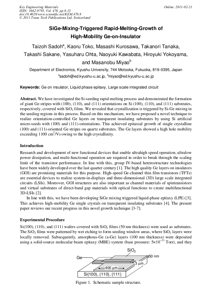
We have investigated the Si-seeding rapid-melting process and demonstrated the formation of giant Ge stripes with (100), (110), and (111) orientations on Si (100), (110), and (111) substrates, respectively, covered with SiO2 films. We revealed that crystallization is triggered by Si-Ge mixing in the seeding regions in this process. Based on this mechanism, we have proposed a novel technique to realize orientation-controlled Ge layers on transparent insulating substrates by using Si artificial micro-seeds with (100) and (111)-orientations. This achieved epitaxial growth of single crystalline (100) and (111)-oriented Ge stripes on quartz substrates. The Ge layers showed a high hole mobility exceeding 1100 cm2/Vs owing to the high crystallinity.

You might also be interested in these eBooks

Info:

Periodical:

Pages:

8-13

Citation:

Online since:

February 2011

Export:

Price:

Permissions CCC:

Permissions PLS:

Сopyright:

© 2011 Trans Tech Publications Ltd. All Rights Reserved

Share:

Citation:

[1] M. Miyao and K. Nakagawa: Jpn. J. Appl. Phys. Vol. 33 (1994), p.3791.

Google Scholar

[2] Y. Ando, K. Hamaya, K. Kasahara,Y. Kishi,K. Ueda, K. Sawano, T. Sadoh, and M. Miyao: Appl. Phys. Lett. Vol. 94 (2009).

DOI: 10.1063/1.3130211

Google Scholar

[3] M. Miyao, T. Tanaka, K. Toko, and M. Tanaka : Appl. Phys. Express Vol. 2 (2009), p.045503.

Google Scholar

[4] M. Miyao, K. Toko, T. Tanaka, and T. Sadoh : Appl. Phys. Lett. Vol. 95 (2009), p.022115.

Google Scholar

[5] M. Kurosawa, N. Kawabata, T. Sadoh, and M. Miyao: Appl. Phys. Lett. Vol. 95 (2009), p.132103.

Google Scholar

[6] K. Toko, T. Sakane, T. Tanaka, T. Sadoh, and M. Miyao: Appl. Phys. Lett. Vol. 95 (2009), p.112107.

DOI: 10.1063/1.3231925

Google Scholar

[7] T. Tanaka, K. Toko, T. Sadoh, and M. Miyao: Appl. Phys. Express, Vol. 3 (2010), p.031301.

Google Scholar

[8] Y. Liu, M. D. Deal, and D. Plummer: Appl. Phys. Lett. Vol. 84 (204), p.2563, D. J. Tweet, J. J. Lee, J. S. Maa, and S. T. Hsu: Appl. Phys. Lett. Vol. 87 (2005).

Google Scholar

[9] M. Tamura, H. Tamura, M. Miyao, and T. Tokuyama: Jpn. J. Appl. Phys. Vol. 20, Suppl. 20-1 (1981), p.43.

Google Scholar

[10] K. Toko, I. Nakao, T. Sadoh, T. Noguchi, and M. Miyao: Solid-State Electron. Vol. 53 (2009), p.1159.

Google Scholar

[11] T. Maeda, K. Ikeda, S. Nakaharai, T. Tezuka, N. Sugiyama, Y. Moriyama, and S. Tkagi: Thin Solid Films Vol. 508 (2006), p.346.

DOI: 10.1016/j.tsf.2005.07.339

Google Scholar