Via Size-Dependent Properties of TiAl Ohmic Contacts on 4H-SiC
p.185
p.185
Engineering the Schottky Interface of 3.3 kV SiC JBS Diodes Using a P2O5 Surface Passivation Treatment
p.190
p.190
The Development of Monolithic Silicon Carbide Intracortical Neural Interfaces for Long-Term Human Implantation
p.195
p.195
Graphite Assisted P and Al Implanted 4H-SiC Laser Annealing
p.204
p.204
A Novel Tool Layout and Process for Single Side Wet Electrochemical Processing of Porous Silicon Carbide Layers without Edge Exclusion
p.209
p.209
Multiscale Simulations of Plasma Etching in Silicon Carbide Structures
p.214
p.214
Optimisation of Ti Ohmic Contacts Formed by Laser Annealing on 4H-SiC
p.219
p.219
Ohmic Contact Formation on 4H-SiC with a Low Thermal Budget by Means of Shallow Phosphorous Ion Implantation
p.224
p.224
Highest Quality and Repeatability for Single Wafer 150mm SiC CMP Designed for High Volume Manufacturing
p.229
p.229
A Novel Tool Layout and Process for Single Side Wet Electrochemical Processing of Porous Silicon Carbide Layers without Edge Exclusion

Abstract:
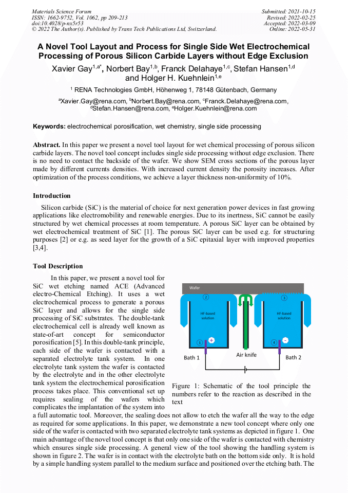
In this paper we present a novel tool layout for wet chemical processing of porous silicon carbide layers. The novel tool concept includes single side processing without edge exclusion. There is no need to contact the backside of the wafer. We show SEM cross sections of the porous layer made by different currents densities. With increased current density the porosity increases. After optimization of the process conditions, we achieve a layer thickness non-uniformity of 10%.
You have full access to the following eBook

Info:
Periodical:
Materials Science Forum (Volume 1062)
Pages:
209-213
DOI:
https://doi.org/10.4028/p-nx5r53
DOI link
Citation:
Online since:
May 2022
Authors:
Permissions:
Share:
Citation: