p.554
p.560
p.565
p.570
p.576
p.582
p.588
p.593
p.598
Impact of Device Design Parameters on 15 kV SiC MOSFETs

Abstract:
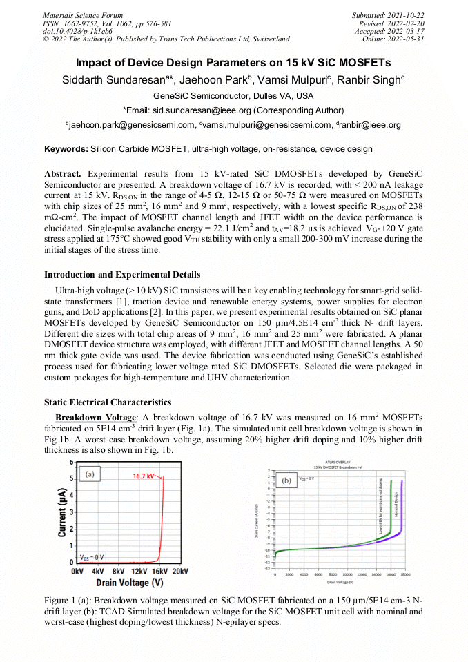
Experimental results from 15 kV-rated SiC DMOSFETs developed by GeneSiC Semiconductor are presented. A breakdown voltage of 16.7 kV is recorded, with < 200 nA leakage current at 15 kV. RDS,ON in the range of 4-5 Ω, 12-15 Ω or 50-75 Ω were measured on MOSFETs with chip sizes of 25 mm2, 16 mm2 and 9 mm2, respectively, with a lowest specific RDS,ON of 238 mΩ-cm2. The impact of MOSFET channel length and JFET width on the device performance is elucidated. Single-pulse avalanche energy = 22.1 J/cm2 and tAV=18.2 μs is achieved. VG-+20 V gate stress applied at 175°C showed good VTH stability with only a small 200-300 mV increase during the initial stages of the stress time.

Info:
Periodical:
Pages:
576-581
DOI:
Citation:
Online since:
May 2022
Authors:
Keywords:
Permissions:
Share:
Citation: