Characterization of Thick 2-Inch 4H-SiC Layers Grown by the Continuous Feed-Physical Vapor Transport Method
p.91
p.91
Effect of Thermal Field on Interface Step Structures during PVT Growth of (0001)Si 6H-SiC
p.95
p.95
Large Diameter and Long Length Growth of SiC Single Crystal
p.99
p.99
Effect of Crucible Design on the Shape and the Quality in 6H-SiC Crystals Grown by Physical Vapor Transport
p.103
p.103
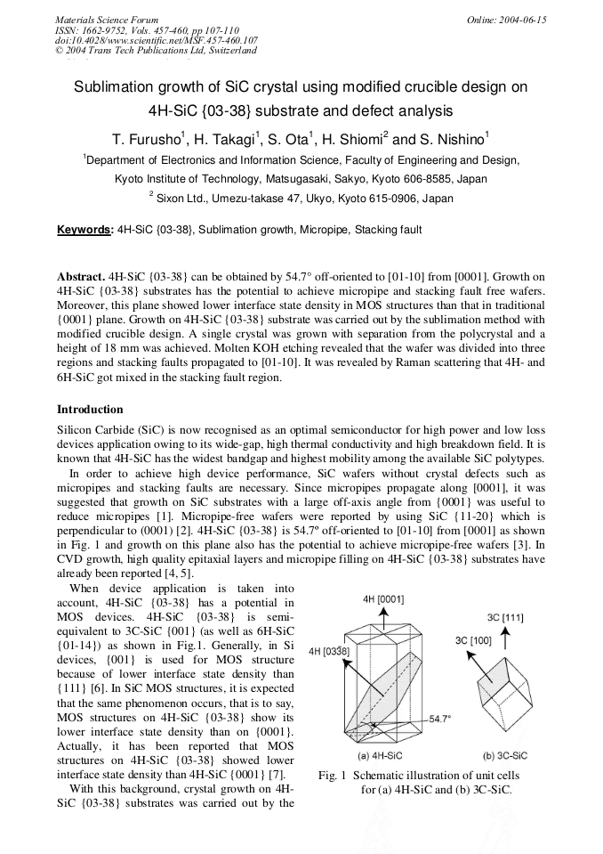
Sublimation Growth of SiC Crystal Using Modified Crucible Design on 4H-SiC {03-38} Substrate and Defect Analysis
p.107
p.107
Natural Crystal Habit and Preferential Growth Directions during PVT of Silicon Carbide
p.111
p.111
High Quality SiC Bulk Growth by Sublimation Method using Elemental Silicon and Carbon Powder as SiC Source Materials
p.115
p.115
Flux Growth of SiC Crystals from Eutectic Melt SiC-B4C
p.119
p.119
Solution Growth of Self-Standing 6H-SiC Single Crystal Using Metal Solvent
p.123
p.123
Sublimation Growth of SiC Crystal Using Modified Crucible Design on 4H-SiC {03-38} Substrate and Defect Analysis

Abstract:
You might also be interested in these eBooks
Info:
Periodical:
Materials Science Forum (Volumes 457-460)
Pages:
107-110
Citation:
Online since:
June 2004
Authors:
Keywords:
Price:
Сopyright:
© 2004 Trans Tech Publications Ltd. All Rights Reserved
Share:
Citation: