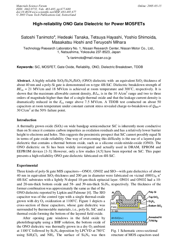
High-Reliability ONO Gate Dielectric for Power MOSFETs

Article Preview

Abstract:

Thin (~10nm) Si layers have been deposited using Rapid Thermal CVD at temperatures ranging 950°C-1050°C. RTCVD deposited Si layers have been oxidized using N2O at 1300°C during relatively short times (15min) to produce SiO2 layers of 20-30nm. The interfacial characteristics of N2O oxidized RTCVD layers have been studied using the conductance method, showing a reduced traps density and a low band bending fluctuation when compared with conventional N2O grown oxides on 4H-SiC substrates. The surface topology of these layers has also been analyzed evidencing an adequate topography with low roughness.

You might also be interested in these eBooks

Info:

Periodical:

Materials Science Forum (Volumes 483-485)

Pages:

677-680

Citation:

Online since:

May 2005

Export:

Price:

Permissions CCC:

Permissions PLS:

Сopyright:

© 2005 Trans Tech Publications Ltd. All Rights Reserved

Share:

Citation:

[1] T. Watanabe, A. Menjoh, T. Mochizuki, S. Shinozaki and O. Ozawa, Proc. IEEE 28th IRPS, (1985), p.18.

Google Scholar

[2] E. Suzuki, H. Higashi, K. Ishii and Y. Hayashi, IEEE Transact. Electron Dev. Vol. ED-30 (1983), p.122.

Google Scholar

[3] G. Samachisa, C. -S. Su, Y. -S. Kao, G. Smarandoiu, S. -Y. M Wang, T. Wong and C. Hu, IEEE J. Solid-State Circuits Vol. SC-22 (1987), p.176.

DOI: 10.1109/jssc.1987.1052799

Google Scholar

[4] L.A. Lipkin and J.L. Palmour, IEEE Transact. Electron Dev. Vol. ED-46 (1999), p.525.

Google Scholar

[5] X.W. Wang, Z.J. Luo and T. -P. Ma, IEEE Transact. Electron Dev. Vol. ED-47 (2000), p.458.

Google Scholar

[6] S. Tanimoto, N. Kiritani, M. Hoshi, H. Okushi and K. Arai, Mater. Sci. Forum Vols. 443-436 (2003), p.725.

Google Scholar

[7] N. Kiritani, M. Hoshi, S. Tanimoto, K. Adachi, S. Nishizawa, T. Yatsuo, H. Okushi and K. Arai, Mater. Sci. Forum Vols. 443-436 (2003), p.669.

DOI: 10.4028/www.scientific.net/msf.433-436.669

Google Scholar