Optimisation of Heterostructure Bipolar Transistors in SiC

Article Preview

Abstract:

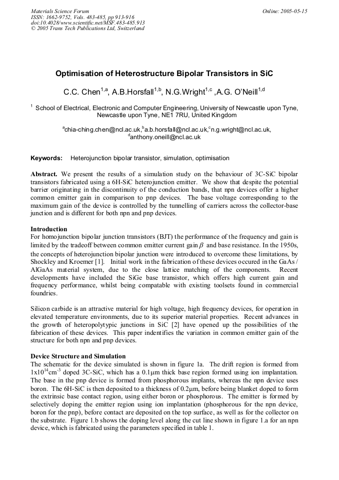
We present the results of a simulation study on the behaviour of 3C-SiC bipolar transistors fabricated using a 6H-SiC heterojunction emitter. We show that despite the potential barrier originating in the discontinuity of the conduction bands, that npn devices offer a higher common emitter gain in comparison to pnp devices. The base voltage corresponding to the maximum gain of the device is controlled by the tunnelling of carriers across the collector-base junction and is different for both npn and pnp devices.

You might also be interested in these eBooks

Info:

Periodical:

Materials Science Forum (Volumes 483-485)

Pages:

913-916

Citation:

Online since:

May 2005

Export:

Price:

Permissions CCC:

Permissions PLS:

Сopyright:

© 2005 Trans Tech Publications Ltd. All Rights Reserved

Share:

Citation:

[1] S.M. Sze, Semiconductor device, Physics and Technology, John Wiley, (2002).

Google Scholar

[2] N.S. Savkina, A.M. Stel'chuk, L.M. Sorokin, et al, Mat. Sci. Forum. Vol. 433-436, (2003), p.293.

Google Scholar

[3] D.M. Caughey, R.E. Thomas, Proceedings of the IEEE, Vol. 55, (1967), p.2192.

Google Scholar

[4] A. Lebedev, A.M. Strel'chuk, D.V. Davydov, et al, Appl. Surf. Sci., Vol. 184, (2001), p.419.

Google Scholar

[5] J.W. Slotboom, H. C . de Graa, Solid State Electronics, Vol. 19, (1976), p.857.

Google Scholar

[6] U. Lindefelt, J. Appl. Phys., Vol. 84, (1998), p.2628.

Google Scholar

[7] M. Yamanaka, H.H. Daimon, E. Sakuma, et al, Jpn.J. Appl. Phys. Vol. 26, (1987), L533.

Google Scholar