p.961
p.965
p.969
p.975
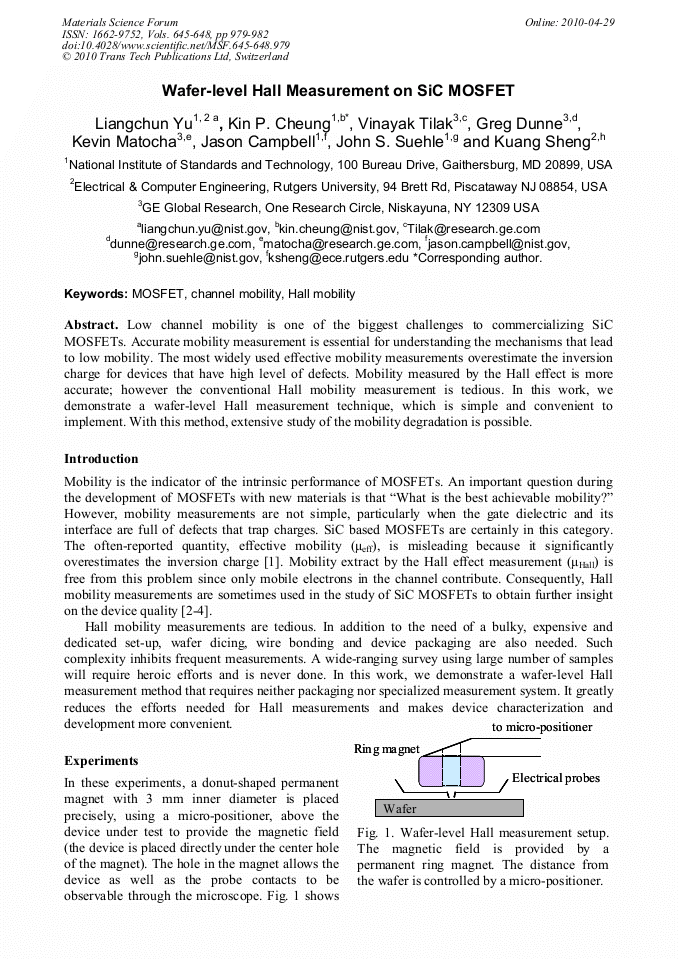
p.979
p.983
p.987
p.991
p.995
Wafer-Level Hall Measurement on SiC MOSFET

Abstract:
Low channel mobility is one of the biggest challenges to commercializing SiC MOSFETs. Accurate mobility measurement is essential for understanding the mechanisms that lead to low mobility. The most widely used effective mobility measurements overestimate the inversion charge for devices that have high level of defects. Mobility measured by the Hall effect is more accurate; however the conventional Hall mobility measurement is tedious. In this work, we demonstrate a wafer-level Hall measurement technique, which is simple and convenient to implement. With this method, extensive study of the mobility degradation is possible.
Info:
Periodical:
Pages:
979-982
Citation:
Online since:
April 2010
Keywords:
Price:
Сopyright:
© 2010 Trans Tech Publications Ltd. All Rights Reserved
Share:
Citation: