p.973
p.977
p.981
p.985
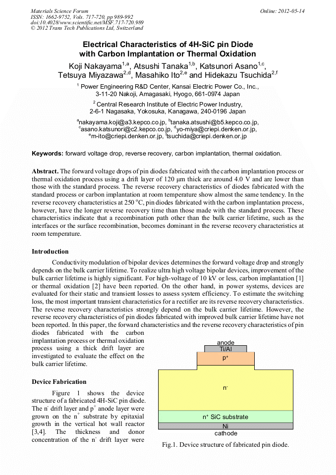
p.989
p.993
p.997
p.1001
p.1005
Electrical Characteristics of 4H-SiC Pin Diode with Carbon Implantation or Thermal Oxidation

Abstract:
The forward voltage drops of pin diodes with the carbon implantation process or thermal oxidation process using a drift layer of 120 μm thick are around 4.0 V and are lower than those with the standard process. The reverse recovery characteristics of diodes with the standard process or carbon implantation at room temperature show almost the same tendency. In the reverse recovery characteristics at 250 oC, pin diodes with carbon implantation process, however, have the longer reverse recovery time than those with the standard process. These characteristics indicate that a recombination path other than the bulk carrier lifetime, such as the interfaces or the surface recombination, becomes dominant in the reverse recovery characteristics at room temperature.

Info:
Periodical:
Pages:
989-992
Citation:
Online since:
May 2012
Price:
Сopyright:
© 2012 Trans Tech Publications Ltd. All Rights Reserved
Share:
Citation: