VF Degradation of 4H-SiC PiN Diodes Using Low-BPD Wafers
p.851
p.851
13-kV, 20-A 4H-SiC PiN Diodes for Power System Applications
p.855
p.855
Variant of Excess Current in 4H-SiC pn Structures
p.859
p.859
The Cryogenic Testing and Characterisation of SiC Diodes
p.863
p.863
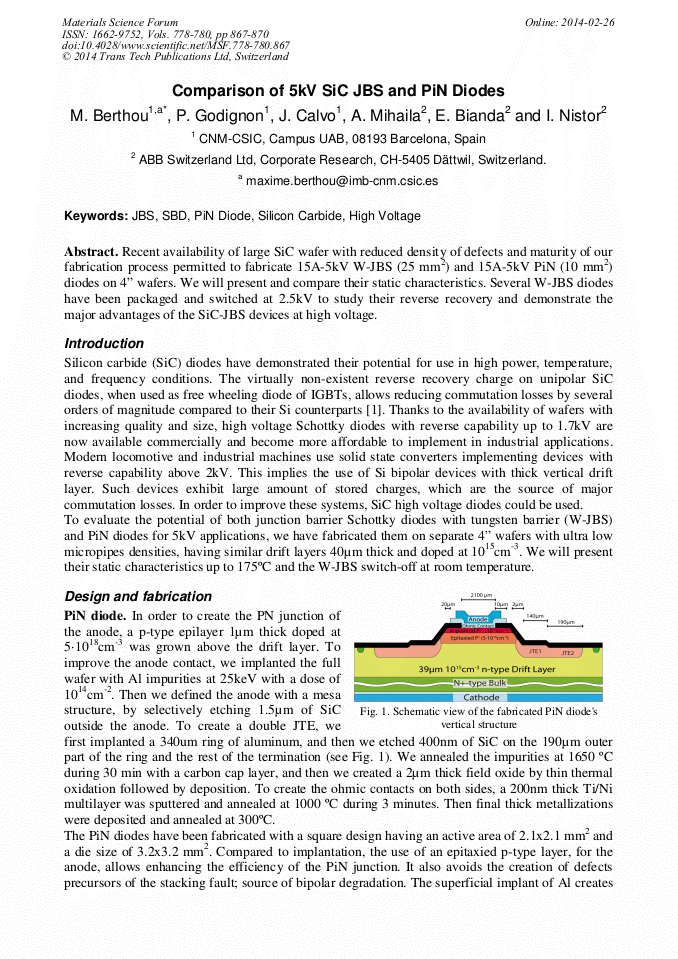
Comparison of 5kV SiC JBS and PiN Diodes
p.867
p.867
650V SiC JFET for High Efficiency Applications
p.871
p.871
Gate-Drive Voltage Design for 600-V Vertical-Trench Normally-Off SiC JFETs toward 94% Efficiency Server Power Supply
p.875
p.875
Evaluation of SiC Stack Cascode for 200°C Operations
p.879
p.879
Beam Acceleration Experiment with SiC Based Power Supply and the Next Generation SiC-JFET Package
p.883
p.883
Comparison of 5kV SiC JBS and PiN Diodes

Abstract:
Recent availability of large SiC wafer with reduced density of defects and maturity of our fabrication process permitted to fabricate 15A-5kV W-JBS (25 mm2) and 15A-5kV PiN (10 mm2) diodes on 4 wafers. We will present and compare their static characteristics. Several W-JBS diodes have been packaged and switched at 2.5kV to study their reverse recovery and demonstrate the major advantages of the SIC-JBS devices at high voltage.
You might also be interested in these eBooks
Info:
Periodical:
Materials Science Forum (Volumes 778-780)
Pages:
867-870
Citation:
Online since:
February 2014
Authors:
Price:
Сopyright:
© 2014 Trans Tech Publications Ltd. All Rights Reserved
Share:
Citation: