p.625
p.629
p.633
p.639
p.643
p.647
p.651
p.655
p.660
Deep Trench Termination Structure with p-Type SiC Layer for Improved Reliability of High Voltage IGBT

Abstract:
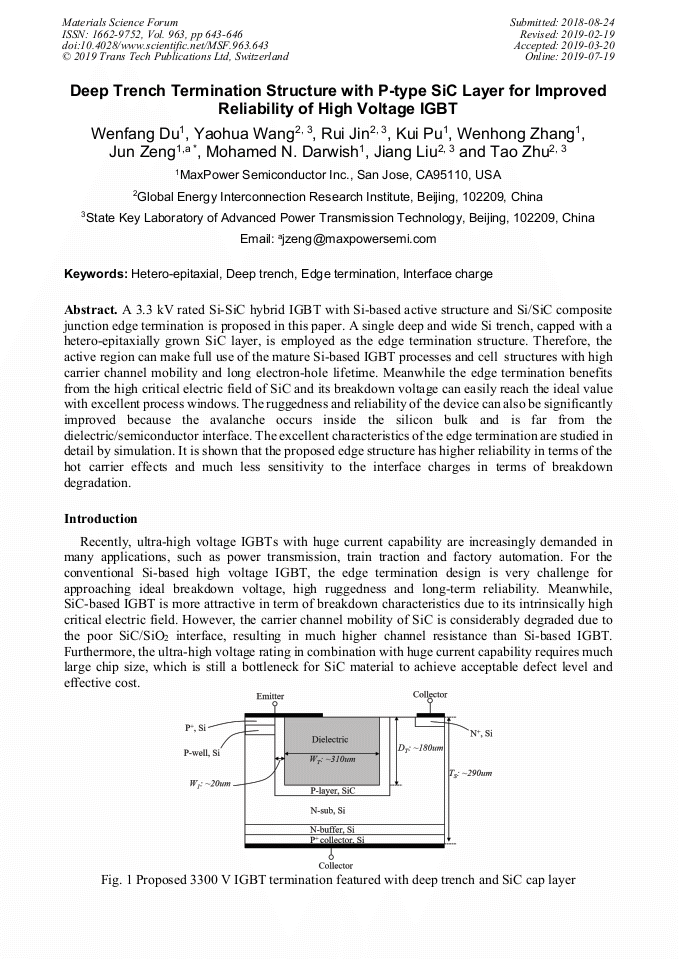
A 3.3 kV rated Si-SiC hybrid IGBT with Si-based active structure and Si/SiC composite junction edge termination is proposed in this paper. A single deep and wide Si trench, capped with a hetero-epitaxially grown SiC layer, is employed as the edge termination structure. Therefore, the active region can make full use of the mature Si-based IGBT processes and cell structures with high carrier channel mobility and long electron-hole lifetime. Meanwhile the edge termination benefits from the high critical electric field of SiC and its breakdown voltage can easily reach the ideal value with excellent process windows. The ruggedness and reliability of the device can also be significantly improved because the avalanche occurs inside the silicon bulk and is far from the dielectric/semiconductor interface. The excellent characteristics of the edge termination are studied in detail by simulation. It is shown that the proposed edge structure has higher reliability in terms of the hot carrier effects and much less sensitivity to the interface charges in terms of breakdown degradation.
Info:
Periodical:
Pages:
643-646
DOI:
Citation:
Online since:
July 2019
Authors:
Keywords:
Price:
Сopyright:
© 2019 Trans Tech Publications Ltd. All Rights Reserved
Share:
Citation: