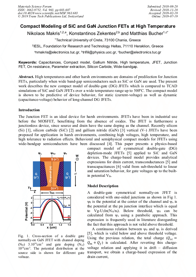
[1]
P. Fernandez-Martinez, D. Flores, S. Hidalgo, D. Quirion, R. Dura, M. Ullan, First fabrication of a silicon vertical JFET for power distribution in high energy physics applications,, Nuclear Inst. and Methods in Physics Research A, 877, 269–277, (2018).
DOI: 10.1016/j.nima.2017.08.043
Google Scholar
[2]
S. Popelka, P. Hazdra, R. Sharma, V. Zahlava, J. Vobecky, Effect of neutron irradiation on high voltage 4H-SiC vertical JFET characteristics: characterization and modeling,, IEEE Trans. Nuclear Science, 61(6), 3030–3036, (2014).
DOI: 10.1109/tns.2014.2358957
Google Scholar
[3]
D. Ji, S. Chowdhury, Design of 1.2 kV power switches with low RON using GaN-based vertical JFET,, IEEE Trans. Electron Devices, 62(8), 2571–2578, (2015).
DOI: 10.1109/ted.2015.2446954
Google Scholar
[4]
E. Santi, K. Peng, H. A. Mantooth, J. L. Hudgins, Modeling of Wide-Bandgap Power Semiconductor Devices—Part II,, IEEE Trans. Electron Devices, 62(2), 434-442, (2015).
DOI: 10.1109/ted.2014.2373373
Google Scholar
[5]
N. Makris, F. Jazaeri, J.-M. Sallese, R. K. Sharma, M. Bucher, Charge-based modeling of long-channel symmetric double-gate junction FETs – Part I: Drain current and transconductances,, IEEE Trans. Electron Devices, 65(7), 2744–2750, (2018).
DOI: 10.1109/ted.2018.2838101
Google Scholar
[6]
N. Makris, F. Jazaeri, J.-M. Sallese, M. Bucher, Charge-based modeling of long-channel symmetric double-gate junction FETs – Part II: Total charges and transcapacitances,, IEEE Trans. Electron Devices, 65(7), 2751–2755, (2018).
DOI: 10.1109/ted.2018.2838090
Google Scholar
[7]
A. Grekov, Z. Chen, E. Santi, J. Hudgins, A. Mantooth, D. Sheridan, J. Casady, Parameter extraction procedure for high power SiC JFET,, IEEE Energy Conversion Congress and Exposition (ECCE), 1466–1471, (2009).
DOI: 10.1109/ecce.2009.5316253
Google Scholar
[8]
E. Platania, Z. Chen, F. Chimento, A. E. Grekov, R. Fu, L. Lu, A. Raciti, J. L. Hudgins, H. A. Mantooth, D. C. Sheridan, J. Casady, E. Santi, A Physics-Based Model for a SiC JFET Accounting for Electric-Field-Dependent Mobility,, IEEE Trans. Industry Applications, 47(1), 199–211, (2011).
DOI: 10.1109/tia.2010.2090843
Google Scholar
[9]
D. E. Ward, R. W. Dutton, A charge-oriented model for MOS transistor capacitances,, IEEE J. Solid-State Circuits, 13(5), 703-708, (1978).
DOI: 10.1109/jssc.1978.1051123
Google Scholar
[10]
S. Banas, J. Dobes, V. Panko, Techniques of JFET gate capacitance modeling,, World Congress on Engineering and Computer Science (WCECS), vol. II, 5 p., (2016).
Google Scholar
[11]
N. Makris; M. Bucher; F. Jazaeri, J.-M. Sallese, JFETlab: An Online Simulation Tool for Double Gate Symmetrical JFETs,, https://nanohub.org/resources/jfetlab, (2018).
Google Scholar
[12]
M. Roschke, F. Schwierz, Electron mobility models for 4H, 6H, and 3C SiC,, IEEE Trans. Electron Devices, 48(7), 1442–1447, (2001).
DOI: 10.1109/16.930664
Google Scholar
[13]
D. Stefanakis, K. Zekentes, TCAD models of the temperature and doping dependence of the bandgap and low field carrier mobility in 4H-SiC,, Microelectronics Engineering, 116, 65–71, (2014).
DOI: 10.1016/j.mee.2013.10.002
Google Scholar