Phonon Confinement and Impurity Doping in Silicon Nanowires Synthesized by Laser Ablation

Article Preview

Abstract:

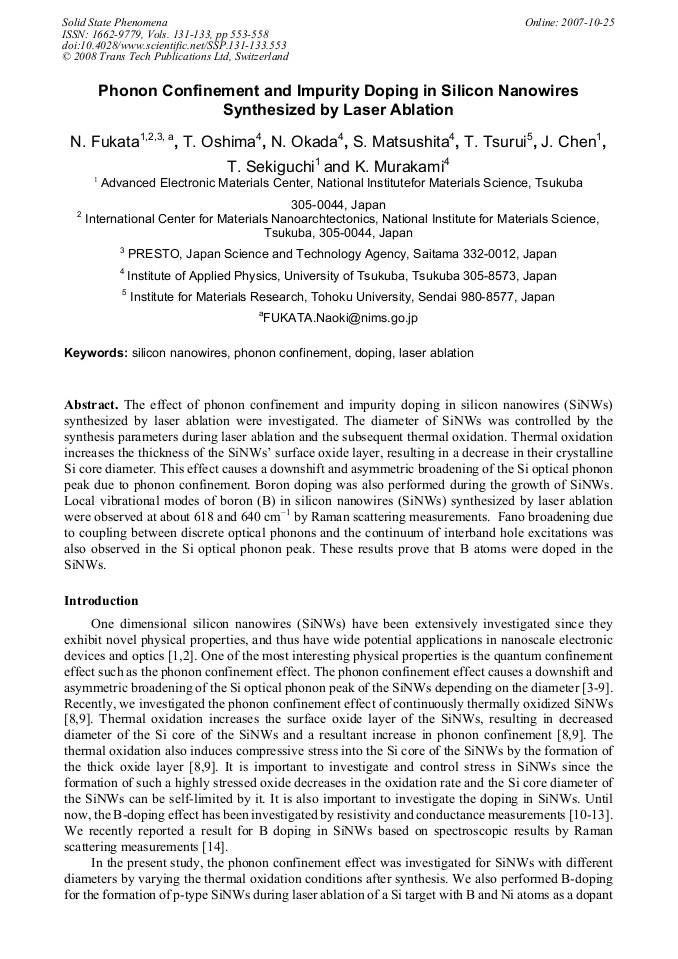
The effect of phonon confinement and impurity doping in silicon nanowires (SiNWs) synthesized by laser ablation were investigated. The diameter of SiNWs was controlled by the synthesis parameters during laser ablation and the subsequent thermal oxidation. Thermal oxidation increases the thickness of the SiNWs’ surface oxide layer, resulting in a decrease in their crystalline Si core diameter. This effect causes a downshift and asymmetric broadening of the Si optical phonon peak due to phonon confinement. Boron doping was also performed during the growth of SiNWs. Local vibrational modes of boron (B) in silicon nanowires (SiNWs) synthesized by laser ablation were observed at about 618 and 640 cm–1 by Raman scattering measurements. Fano broadening due to coupling between discrete optical phonons and the continuum of interband hole excitations was also observed in the Si optical phonon peak. These results prove that B atoms were doped in the SiNWs.

You might also be interested in these eBooks

Info:

Periodical:

Solid State Phenomena (Volumes 131-133)

Pages:

553-558

Citation:

Online since:

October 2007

Export:

Price:

Permissions CCC:

Permissions PLS:

Сopyright:

© 2008 Trans Tech Publications Ltd. All Rights Reserved

Share:

Citation:

[1] A. M. Morales and C. M. Lieber, Science 279, 208 (1998).

Google Scholar

[2] X. Duan, C. Niu, V. Sahi, J. Chen, J. W. Parce, S. Empedocles, and J. L. Goldman, Nature (London) 425, 274 (2003).

DOI: 10.1038/nature01996

Google Scholar

[3] H. Richter, Z. P. Wang, and L. Ley, Solid State Commun. 39, 625 (1981).

Google Scholar

[4] I. H. Campbell and P. M. Fauchet, Solid State Commun. 58, 739 (1986).

Google Scholar

[5] S. Piscanec, M. Cantoro, A.C. Ferrari, J. A. Zapien, Y. Lifshitz, S. T. Lee, S. Hofmann, and J. Robertson, Phys. Rev. B 68, 241312(R) (2003).

DOI: 10.1103/physrevb.68.241312

Google Scholar

[6] S. Bhattachayya and S. Samui, Appl. Phys. Lett. 84, 1564 (2004).

Google Scholar

[7] K. W. Adu, H. R. Gutierrez, U. J. Kim, G. U. Sumanasekera, nad P. C. Eklund, Nano Lett. 5, 400 (2005).

Google Scholar

[8] N. Fukata, T. Oshima, K. Murakami, T. Kizuka, T. Tsurui, and S. Ito, Appl. Phys. Lett. 86, 213112 (2005).

DOI: 10.1063/1.1931055

Google Scholar

[9] N. Fukata, T. Oshima, N. Okada, T. Kizuka, T. Tsurui, S. Ito and K. Murakami, J. Appl. Phys. 100 (2), 024311 (2006).

DOI: 10.1063/1.2218386

Google Scholar

[10] Y. Cui, X. Duan, J. Hu, and C. M. Lieber, J. Phys. Chem. B104, 5213 (2000).

Google Scholar

[11] D. D. D. Ma, C. S. Lee, and S. T. Lee, Appl. Phys. Lett. 79, 2468 (2001).

Google Scholar

[12] K. K. Lew, L. Pan, T. E. Bogart, S. M. Dilts, E. C. Dickey, J. M. Redwing, Y. Wang, M. Cabassi, T. S. Mayer, and S. W. Novak, Appl. Phys. Lett. 85, 3101 (2004).

DOI: 10.1063/1.1792800

Google Scholar

[13] L. Pan, K. K. Lew, J. M. Redwing, and E. C. Dickey, J. Crystal Growth 277, 428 (2005).

Google Scholar

[14] N. Fukata, J. Chen, T. Sekiguchi, N. Okada, K. Murakami, T. Tsurui, and S. Ito, Appl. Phys. Lett. 89, 203109 (2006).

DOI: 10.1063/1.2372698

Google Scholar

[15] R.S. Wagner and W.C. Ellis, Appl. Phys. Lett. 4, 89 (1964).

Google Scholar

[16] N. Fukata, T. Oshima, T. Tsurui, S. Ito and K. Murakam, Sci. Tech. Adv. Mater. 6, 628 (2005).

Google Scholar

[17] S. Piscanec, M. Cantro, A. C. Ferrari, J. A. Zapien, Y. Lifshitz, S. T. Lee, S. Hofmann, and J. Robertson, Phys. Rev. B 68, 241312 (2003).

Google Scholar

[18] U. Fano, Phys. Rev. 124, 1866 (1961).

Google Scholar

[19] C. P. Herrero and M. Stutzmann, Phys. Rev. B 38, 12668 (1988).

Google Scholar

[20] M. Chandrasekhar, H. R. Chandrasekhar, M. Grimsditch, and M. Cardona, Phys. Rev. B22, 4825 (1980). REVISED VERSION October (2007).

Google Scholar